
Instruction Manual
5
5
4
4
3
3
2
2
1
1
D D
C C
B B
A A
Notes:
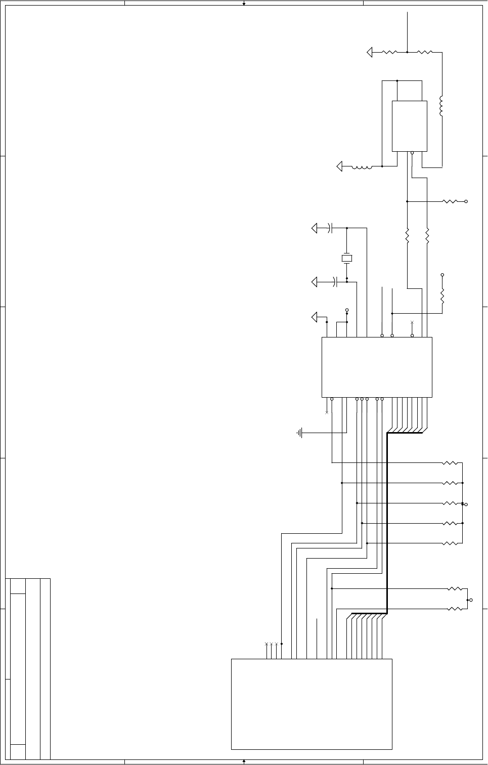
-EP9312 symbol is incomplete as this is meant
only for reference purposes.
-SENSE/EOT signal acts as both a USB Vbus detect
AND the end-of-transfer signal for DMA operations.
This is intentional. Please see the Philips PDIUSBD12
datasheet for additional details.
-Likewise, R10/R11 form a 3.3V pullup network for the EOT
signal via the USB +5V bus rail. Thus, there is no pullup resistor
for the SENSE/EOT signal.
-This schematic assumes minimal or no loading of the buses
between the EP9312 and the PDIUSBD12. Depending on your
design, you may need additional buffering to reduce
the overall load on these signals.
<Doc> 0
EP9312 USB 1.1 Slave
B
11Tuesday, June 24, 2003
Title
Size Document Number Rev
Date: Sheet
of
INT1
DREQ
INT1
DA3
DA6
SENSE/EOT
DA5
DA7
DA7
DA6
DA1
DA4
DREQ
DA0
DA5
DA2
DA4
SENSE/EOT
DA2
DA1
DA0
DA3
DA[7:0]
VCC3
VCC3
VCC3
VCC3
VCC3
L1
FERRITE_BEAD, 0603
1 2
P1
USB-B
1
2
3
46
5
PWR
D-
D+
GNDSHIELD
SHIELD
R9
1.5K, 0603
12
EP9312-D partial SRAM interface
U5
DA0
DA1
DA2
DA3
DA4
DA5
DA6
DA7
EGPIO7/DREQ0
EGPIO8/DACK0
EGPIO9/DEOT0
INT1
/CS7
/RD
/WR
AD0
AD1
AD2
AD3
C11
22PF, 0603
12
C12
22PF, 0603
12
R1
4.7K
12
R2
4.7K
12
R3
4.7K
12
R12
4.7K
12
R4
4.7K
12
R7
4.7K
12
X2
6MHZ, HC49-US
12
R8
4.7K
12
R11
1M, 0603
12
R10
560K, 0603
12
R159
4.7K, 0603
12
U3
PDIUSBD12, TSSOP28
1
2
3
4
6
7
8
9
11
15
16
10
28
22
23
18
19
20
5
24
25
26
21
27
17
12
14
D0
D1
D2
D3
D4
D5
D6
D7
*CS
*RD
*WR
ALE
A0
XTAL1
XTAL2
*DMACK
*EOT
*RST
GND
VCC
D-
D+
*GL
V3.3
*DMREQ
SUSPEND
*INT
R5
18.2_1%, 0603
12
R6
18.2_1%, 0603
12
L2
FERRITE_BEAD, 0603
1 2