
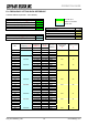
Specifications

.
OG_STD-302N-R_v15e Circuit Design, Inc.
12
OPERATION GUIDE
Method of serial data input to the PLL
After the RF channel table plan is decided, the data needs to be allocated to the ROM table and read from
there or calculated with the software.
Together with this setting data, operation bits that decide operation of the PLL must be sent to the PLL.
The operation bits for setting the PLL are as follows. These values are placed at the head of the reference
counter value and are sent to the PLL.
1. CS: Charge pump current select bit
CS = 0 +/-1.5 mA select VCO is optimized to +/-1.5 mA
2. LDS: LD/fout output setting bit
LDS = 0 LD select Hardware is set to LD output
3. FC: Phase control bit for the phase comparator
FC = 1 Hardware operates at this phase
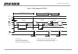
The PLL IC, which operates as shown in the block diagram in the manual, shifts the data to the 19-bit shift
register and then transfers it to the respective latch (counter, register) by judging the CNT control bit value
input at the end.
1. CLK [Clock]: Data is shifted into the shift register on the rising edge of this clock.
2. LE [Load Enable]: Data in the 19-bit shift register is transferred to respective latches on the rising edge of
the clock. The data is transferred to a latch according to the control bit CNT value.
3. Data [Serial Data]: You can perform either reference counter setup or programmable counter setup first.
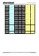
CS
Invalid Data
LDS FC SW
R14 R13 CNT=1
R1
1st data
2nd data N11 N10 N9 N8 N7 N6 CNT=0A1
1st Data 2nd Data
DATA
CLK
LE
MSB LSB
t6
t5t4
t3t2t1
t0
#: t0,t5 >= 100 ns t1,t2,t6 >= 20 ns t3,t4 >= 30 ns
#: Keep the LE terminal at a low level, w hen w rite the data to the shift resister.
STD-302
terminal name
Figure 2