OPERATION GUIDE UHF Narrow band radio transceiver STD-302N-R 434MHz Operation Guide Version 1.5 (Feb. 2014) CIRCUIT DESIGN, INC., 7557-1 Hotaka, Azumino Nagano 399-8303 JAPAN Tel: + +81-(0)263-82-1024 Fax: + +81-(0)263-82-1016 e-mail: info@circuitdesign.jp http://www.cdt21.
OPERATION GUIDE CONTENTS GENERAL DESCRIPTION & FEATURES ...........................3 SPECIFICATIONS STD-302N-R 434 MHz .......................4 PIN DESCRIPTION .............................................................6 BLOCK DIAGRAM...............................................................8 DIMENSIONS......................................................................9 PLL IC CONTROL .............................................................10 PLL IC control ................................
OPERATION GUIDE GENERAL DESCRIPTION & FEATURES General Description The UHF FM narrow band semi-duplex radio data module STD-302N-R is a R&TTE and RoHS compliant, high performance transceiver designed for use in industrial applications requiring long range, high performance and reliability. All high frequency circuits are enclosed inside a robust housing to provide superior resistance against shock and vibration.
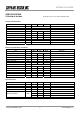
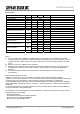
OPERATION GUIDE SPECIFICATIONS STD-302N-R 434 MHz All ratings at 25 +/-10 °C unless otherwise noted General characteristics Item Applicable standard Communication method Emission class Operating frequency range Operation temperature range Storage temperature range Aging rate Initial frequency tolerance Dimensions Weight Units MHz °C °C ppm ppm mm g MIN TYP MAX EN 300 220 Simplex, Half-duplex F1D 433.050 434.775 -20 60 -30 75 -1 1 -1.5 1.
OPERATION GUIDE Receiver part Item Receiver type 1st IF frequency 2nd IF frequency Maximum input level BER (0 error/2556 bits) *1 BER (1 % error) *2 Sensitivity 12dB/ SINAD MHz kHz dBm dBm dBm dBm Spurious response rejection *3 dB Adjacent CH selectivity *3 Intermodulation *4 DO output level dB dB V RSSI rising time ms Time until valid Data-out *5 ms Spurious radiation dBm RSSI mV MIN TYP MAX Double superheterodyne 21.7 450 10 -107 -110 -116 -119 80 60 50 50 0 2.
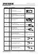
OPERATION GUIDE PIN DESCRIPTION Pin name I/O Description Equivalent circuit 47P SAW FILTER RF I/O RF RF input terminal Antenna impedance nominal 50 Ω 100nH GND GND I GROUND terminal The GND pins and the feet of the shield case shoud be connected to the wide GND pattern. VCC 2.8V VCC TXSEL I Power supply terminal DC 3.0 to 5.5 V I TX select terminal GND = TXSEL active To enable the transmitter circuits, connect TXSEL to GND and RXSEL to OPEN or 2.8 V.
OPERATION GUIDE 2.8V LD O PLL lock/unlock monitor terminal Lock = H (2.8 V), Unlock = L (0 V) 2K LD MB15E03 102 RSSI O Received Signal Strength Indicator terminal 2.8V DO DI O I OG_STD-302N-R_v15e Data output terminal Interface voltage: H=2.8V, L=0V 10K 2K DO 102 Data input terminal Interface voltage: H=2.8V to Vcc, L=0V Input data pulse width Min.100 μs Max. 15 ms 7 Circuit Design, Inc.
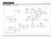
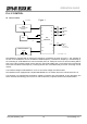
OPERATION GUIDE. BLOCK DIAGRAM OG_STD-302N-R_v15e 8 Circuit Design, Inc.
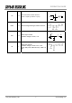
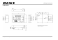
OPERATION GUIDE. DIMENSIONS OG_STD-302N-R_v15e 9 Circuit Design, Inc.
OPERATION GUIDE . PLL IC CONTROL PLL IC control Figure 1 up to 1200MHz VCO 2kohm Voltage Controled Oscillator Fin CLK Xf in Data 2kohm 2kohm LE GND LPF PLL Do +2.8v LE PS VCC ZC 2kohm 21.25MHz DATA MB15E03SL Vp Reference Oscillator CLK LD/f out OSCout P OSCin R LD STD-302 Control pin name #:Control v oltage = +2.8v STD-302N-R is equipped with an internal PLL frequency synthesizer as shown in Figure 1.
OPERATION GUIDE . How to calculate the setting values for the PLL register The PLL IC manual shows that the PLL frequency setting value is obtained with the following equation.
OPERATION GUIDE . Method of serial data input to the PLL After the RF channel table plan is decided, the data needs to be allocated to the ROM table and read from there or calculated with the software. Together with this setting data, operation bits that decide operation of the PLL must be sent to the PLL. The operation bits for setting the PLL are as follows. These values are placed at the head of the reference counter value and are sent to the PLL. 1. CS: Charge pump current select bit CS = 0 +/-1.
OPERATION GUIDE . TIMING CHART Control timing in a typical application is shown in Figure 3. Initial setting of the port connected to the radio module is performed when power is supplied by the CPU and reset is completed. MOS-FET for supply voltage control of the radio module, RXSEL and TXSEL are set to inactive to avoid unwanted emissions. The power supply of the radio module is then turned on.
OPERATION GUIDE Figure 3: Timing diagram for STD-302 Status immediately after pow er comes on. Normal status Channel change No channel change CPU Pow er on STD-302 Pow er on #:3 Receiv e mode Receiv e mode Receiv e mode activ e period activ e period activ e period Activ e period RXSEL CPU control, CH change & Data rec.
OPERATION GUIDE PLL FREQUENCY SETTING DATA REFERENCE 434 MHz ISM band (433.050 - 434.790 MHz) Parameter name Phase Comparing Frequency Fcomp [kHz] Start Channel Frequency Fch [MHz] Channel Step Frequency [kHz] Number of Channel Prescaler M Parameter name Reference Frequency Fosc [MHz] Offset Frequency Foffset [MHz] No. Value : For data input 25 433.0750 25 69 64 : Result of calculation : Fixed value Parameter name Reference Counter R Programmable Counter N Min. Value Programmable Counter N Max.
OPERATION GUIDE 33 34 35 36 37 38 39 40 41 42 43 44 45 46 47 48 49 50 51 52 53 54 55 56 57 58 59 60 61 62 63 64 65 66 67 68 OG_STD-302N-R_v15e 433.9000 433.9250 433.9500 433.9750 434.0000 434.0250 434.0500 434.0750 434.1000 434.1250 434.1500 434.1750 434.2000 434.2250 434.2500 434.2750 434.3000 434.3250 434.3500 434.3750 434.4000 434.4250 434.4500 434.4750 434.5000 434.5250 434.5500 434.5750 434.6000 434.6250 434.6500 434.6750 434.7000 434.7250 434.7500 434.7750 412.2000 412.2250 412.2500 412.2750 412.
OPERATION GUIDE TEST DATA RSSI typical output level characteristic (Purple line) Measurement frequency: 434MHz / Modulation: unmodulated 25°C +/- 5°C 800 RSSI vs dBm mV 700 600 500 400 300 MIN 200 RSSI(mV) MAX 100 dBm 0 -120 -115 -110 -105 -100 -95 -90 -85 -80 -75 -70 -65 -60 -55 -50 -45 -40 -35 -30 -25 -20 Sig (dBm) -120 -115 -110 -105 -100 -95 -90 -85 -80 -75 -70 -65 -60 -55 -50 -45 -40 -35 -30 -25 -20 MIN 134 168 202 238 270 306 346 380 410 444 482 516 558 586 596 596 598 600 600 600 600 OG_STD-3
OPERATION GUIDE Regulatory compliance information Regulatory compliance of the STD-302N-R The STD-302N-R is designed for embedding in other equipment. (Products incorporating the STD-302N-R are henceforward referred to as final products.) The European regulation applicable to the STD-302N-R is the R&TTE Directive 1999/5/EC.The conformity assessment for the STD-302N-R was completed in accordance with the R&TTE Directive Annex III procedures, and the Declaration of Conformity is attached to this manual.
OPERATION GUIDE OG_STD-302N-R_v15e 19 Circuit Design, Inc.
OPERATION GUIDE Important notice Customers are advised to consult with Circuit Design sales representatives before ordering. Circuit Design believes the provided information is accurate and reliable. However, Circuit Design reserves the right to make changes to this product without notice. Circuit Design products are neither designed nor intended for use in life support applications where malfunction can reasonably be expected to result in significant personal injury to the user.
OPERATION GUIDE REVISION HISTORY Version 1.0 1.1 1.2 1.3 1.4 1.5 Date Jun. 2006 Feb. 2007 Oct. 2007 May 2008 Aug. 2013 Feb. 2014 OG_STD-302N-R_v15e Description STD-302N-R 434MHz The first issue Correction Page 6 AF IO status “I” -> “O” Replace drawing of product Page 9 Addition of note to the page 18 and update of DOC DOC updated DOC updated 21 Remark Page 18,19 Page 19 Page 19 Circuit Design, Inc.