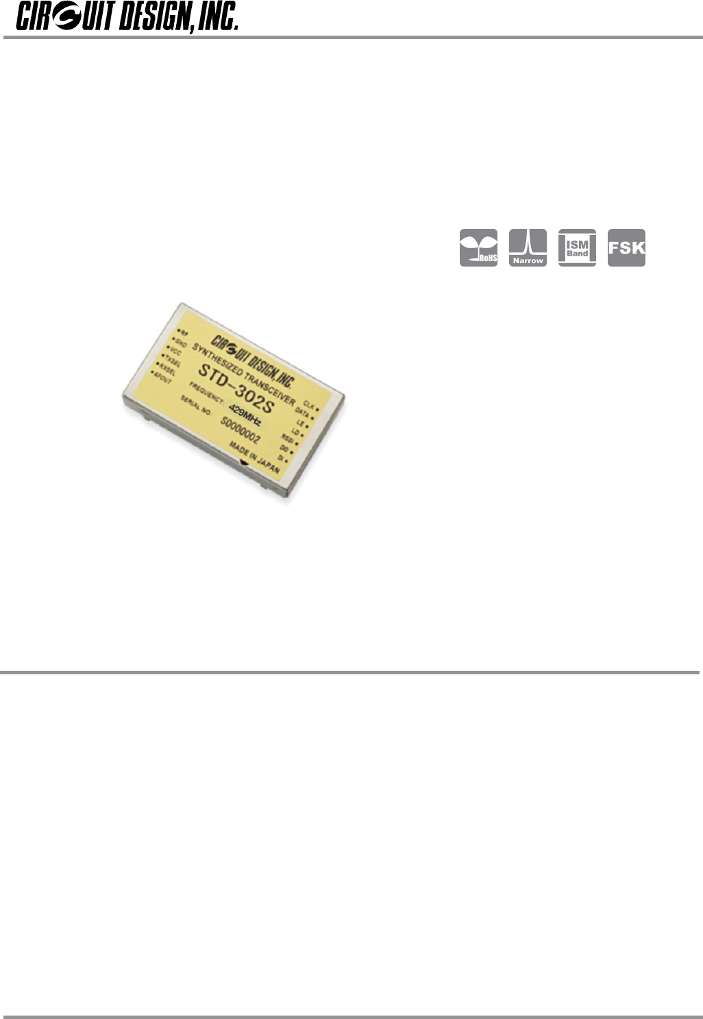
OPERATION GUIDE UHF Narrow band radio transceiver STD-302S 429 MHz Operation Guide Version 1.1 (Apr. 2015) This product requires electrical and radio knowledge for setup and operation. To ensure proper and safe operation, please read this operation guide thoroughly prior to use. Please keep this operation guide for future reference. CIRCUIT DESIGN, INC., 7557-1 Hotaka, Azumino Nagano 399-8303 JAPAN Tel: + +81-(0)263-82-1024 Fax: + +81-(0)263-82-1016 e-mail: info@circuitdesign.jp http://www.
OPERATION GUIDE CONTENTS GENERAL DESCRIPTION & FEATURES ...........................3 SPECIFICATIONS STD-302S 429 MHz ...........................4 PIN DESCRIPTION .............................................................6 BLOCK DIAGRAM...............................................................9 DIMENSIONS....................................................................10 PLL IC CONTROL ............................................................. 11 PLL IC control ..............................
OPERATION GUIDE GENERAL DESCRIPTION & FEATURES General Description The UHF FM narrow band semi-duplex radio data module STD-302S is a high performance transceiver designed for use in industrial applications requiring long range, high performance and reliability. All high frequency circuits are enclosed inside a robust housing to provide superior resistance against shock and vibration. A narrow band technique enables high interference rejection and concurrent operation with multiple modules.
OPERATION GUIDE SPECIFICATIONS STD-302S 434 MHz All ratings at 25 +/-10 °C unless otherwise noted General characteristics Item Communication method Emission class Operating frequency range Operation temperature range Storage temperature range Frequency drift / year Initial frequency tolerance Dimensions Weight Units MHz °C °C ppm ppm mm g MIN TYP MAX Simplex, Half-duplex F1D 429.25 429.7375 -20 60 -30 75 -1 1 -1.5 1.5 30 x 50 x 9 mm 25 g Remarks No dew condensation No dew condensation TX freq.
OPERATION GUIDE Receiver part Item Receiver type 1st IF frequency 2nd IF frequency Maximum input level BER (0 error/2556 bits) *1 BER (1 % error) *2 Sensitivity 12dB/ SINAD MHz kHz dBm dBm dBm dBm MIN TYP MAX Double superheterodyne 21.7 450 10 -108 -115 -120 -120 70 55 30 50 50 70 2.8 50 70 100 120 PN 9 4800bps PN 9 4800bps fm1 k/ dev 2kHz CCITT 1 st Mix, 2 signal method, 1 % error 2 nd Mix, 2 signal method, 1 % error +/- 12.5kHz, 2 signal method, 1 % error 2 signal method, 1 % error L = GND H = 2.
OPERATION GUIDE PIN DESCRIPTION Pin name I/O Description Equivalent circuit RF I/O RF input terminal Antenna impedance nominal 50 Ω GND I GROUND terminal The GND pins and the feet of the shield case should be connected to a wide GND plane. VCC I Power supply terminal DC 3.0 to 5.5 V I TX select terminal GND = TXSEL active To enable the transmitter circuits, connect TXSEL to GND and RXSEL to OPEN or 2.8 V.
OPERATION GUIDE LE I Load enable signal input terminal for PLL data setting input Interface voltage H = 2.8 V, L = 0 V LD O PLL lock/unlock indicator terminal Lock = H (2.8 V), Unlock = L (0 V) RSSI O DO O Data output terminal Interface voltage: H=2.8V, L=0V I Data input terminal Interface voltage: H=2.8V to Vcc, L=0V Input data pulse width Min.200 μs Max. 20 ms DI Received Signal Strength Indicator terminal OG_STD-302S-429M_v11e 7 Circuit Design, Inc.
OPERATION GUIDE FREQUENCY TABLE (STD-T67) Channel number 1 2 3 4 5 6 7 8 9 10 11 12 13 14 15 16 17 18 19 20 21 22 23 24 25 26 27 28 29 30 31 32 33 34 35 36 37 38 39 40 41 42 43 44 45 46 OG_STD-302S-429M_v11e Operating frequency (MHz) 429.1750 429.1875 429.2000 429.2125 429.2250 429.2375 429.2500 429.2625 429.2750 429.2875 429.3000 429.3125 429.3250 429.3750 429.3875 429.3625 429.3750 429.3875 429.4000 429.4125 429.4250 429.4375 429.4500 429.4625 429.4750 429.4875 429.5000 429.5125 429.5250 429.5375 429.
OPERATION GUIDE. BLOCK DIAGRAM OG_STD-302S-429M_v11e 9 Circuit Design, Inc.
OPERATION GUIDE. DIMENSIONS OG_STD-302S-429M_v11e 10 Circuit Design, Inc.
OPERATION GUIDE . PLL IC CONTROL PLL IC control Figure 1 up to 1200MHz VCO 2kohm Voltage Controled Oscillator Fin CLK Xf in Data 2kohm 2kohm GND LPF LE PLL Do +2.8v LE PS VCC ZC 2kohm 21.25MHz DATA MB15E03SL Vp Reference Oscillator CLK LD/f out OSCout P OSCin R LD STD-302 Control pin name #:Control v oltage = +2.8v STD-302S is equipped with an internal PLL frequency synthesizer as shown in Figure 1.
OPERATION GUIDE . How to calculate the setting values for the PLL register The PLL IC manual shows that the PLL frequency setting value is obtained with the following equation.
OPERATION GUIDE . Method of serial data input to the PLL After the RF channel table plan is decided, the data needs to be allocated to the ROM table and read from there or calculated with the software. Together with this setting data, operation bits that decide operation of the PLL must be sent to the PLL. The operation bits for setting the PLL are as follows. These values are placed at the head of the reference counter value and are sent to the PLL. 1. CS: Charge pump current select bit CS = 0 +/-1.
OPERATION GUIDE . TIMING CHART Control timing in a typical application is shown in Figure 3. Initial setting of the port connected to the radio module is performed when power is supplied by the CPU and reset is completed. MOS-FET for supply voltage control of the radio module, RXSEL and TXSEL are set to inactive to avoid unwanted emissions. The power supply of the radio module is then turned on.
OPERATION GUIDE . Figure 3: Timing diagram for STD-302 Status immediately after pow er comes on. Normal status Channel change No channel change CPU Pow er on STD-302 Pow er on #:3 Receiv e mode Receiv e mode Receiv e mode activ e period activ e period activ e period Activ e period RXSEL CPU control, CH change & Data rec.
OPERATION GUIDE PLL FREQUENCY SETTING DATA REFERENCE 429 MHz ISM band (429.1750 – 429.7375 MHz) Parameter name Phase Comparing Frequency Fcomp [kHz] Start Channel Frequency Fch [MHz] Channel Step Frequency [kHz] Number of Channel Prescaler M Parameter name Reference Frequency Fosc [MHz] Offset Frequency Foffset [MHz] Value : For data input 12.5 429.1750 12.5 46 64 : Result of calculation : Fixed value Parameter name Reference Counter R Programmable Counter N Min. Value Programmable Counter N Max.
OPERATION GUIDE 34 35 36 37 38 39 40 41 42 43 44 45 46 429.5875 429.6000 429.6125 429.6250 429.6375 429.6500 429.6625 429.6750 429.6875 429.7000 429.7125 429.7250 429.7375 OG_STD-302S-429M_v11e 407.8875 407.9000 407.9125 407.9250 407.9375 407.9500 407.9625 407.9750 407.9875 408.0000 408.0125 408.0250 408.0375 407.8875 407.9000 407.9125 407.9250 407.9375 407.9500 407.9625 407.9750 407.9875 408.0000 408.0125 408.0250 408.
OPERATION GUIDE TEST DATA RSSI output level characteristic Measurement frequency: 429 MHz / Modulation: unmodulated 25°C +/- 5°C Signal level (dBm) -130 -120 -110 -100 -90 -80 -70 -60 -50 -40 -30 -20 -10 0 OG_STD-302S-429M_v11e RSSI (mV) 130 177 243 288 347 405 460 523 550 552 552 552 552 552 Measurement is done with the PLL setting control board prepared by Circuit Design. 18 Circuit Design, Inc.
OPERATION GUIDE Important notice Customers are advised to consult with Circuit Design sales representatives before ordering. Circuit Design believes the provided information is accurate and reliable. However, Circuit Design reserves the right to make changes to this product without notice. Circuit Design products are neither designed nor intended for use in life support applications where malfunction can reasonably be expected to result in significant personal injury to the user.
OPERATION GUIDE REVISION HISTORY Version 1.0 1.1 Date Jan. 2015 Apr. 2015 OG_STD-302S-429M_v11e Description Remark RSSI graph was revised (P.18) 20 Circuit Design, Inc.