
User's Manual


.
OG_LMD-400-R_v09e Circuit Design, Inc.
14
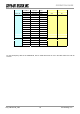
OPERATION GUIDE
Receiv e mode
RXSEL
STD-302
Po w e r o n
TXSEL
CPU c ontr ol,
CH change
&
Data rec.
Timing
Data transmit
#:6 10 to 20 ms later, the receiver can receive the data after changing the channel.
Data #:6
LD
CH
CH
Data #:7
5 ms
10 to 20 ms
#:4 RFchannel change must be performed in receiving mode.
#:7 5 ms later, the data can be received if the RF channel is not changed.
5 ms
#:4
40 ms
CPU
Po w e r o n
CH Data #:5
5 ms
5 ms
Check LD signal
Check LD signal
Normal statusStatus immediately after pow er comes on.
Channel change No channel change
#:4
#:2 Initialize the port connected to the module.
#:3 Supply pow er to the module af ter initializing CPU.
#:1 Reset control CPU
#:1 #:2
#:4
#:3
#:5 40 ms later, the receiver can receive the data after changing the channel..
Figure 3: Timing diagram for STD-302
activ e period
Receiv e mode
activ e period
Receive mode
activ e period
Transm it m ode
activ e
Check LD signal
Activ e period
Transm it mode
activ e
Transm it mode
activ e
LMD-400