
Specifications
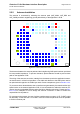

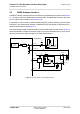


Table Of Contents
- Contents
- Tables
- Figures
- 1 Introduction
- 2 Interface Characteristics
- 2.1 Application Interface
- 2.2 RF Antenna Interface
- 2.3 GNSS Antenna Interface
- 2.4 Sample Application
- 3 Operating Characteristics
- 4 Mechanical Dimensions, Mounting and Packaging
- 5 Regulatory and Type Approval Information
- 6 Document Information
- 7 Appendix

Cinterion
®
PLSx3 Hardware Interface Description
2.3 GNSS Antenna Interface
60
t PLSx3_HID_v01.003 2021-03-12
Public / Released
Page 57 of 121
2.3 GNSS Antenna Interface
In addition to the RF antenna interface PLSx3 also has a GNSS antenna interface. See Section
2.1.1 to find out where the GNSS antenna pad is located. The GNSS pad’s shape is the same
as for the RF antenna interface (see Section 2.2.2).
It is possible to connect active or passive GNSS antennas. In either case they must have 50
impedance. The simultaneous operation of GSM/UMTS/LTE and GNSS is implemented. For
electrical characteristics see Section 2.2.
PLSx3 provides the signal VGNSS to enable an active GNSS antenna power supply. Figure 20
shows the flexibility in realizing the power supply for an active GNSS antenna by giving a sam-
ple circuit realizing the supply voltage for an active GNSS antenna.
Figure 20: Supply voltage for active GNSS antenna
V
GNSS
Active GNSS
Antenna
DC
+
-
Current Sensor
FAN4010
Is
Rs
(3.2V)
Io
Rv
Io
ADCx_IN
Rg
Ug
GNSS
Receiver
Antenna
Matching
RF
DC
ANT_GNSS_DC
ANT_GNSS
Module
Application:
3k3
1u
10k
ESD
Protection
LNA
100
1R0
LDO
BATT+
EN
IN OUT
VGNSS
LP3985IM5-3.2
10k
Si1023X_1
Si1023X_2