
Specifications


Table Of Contents
- Contents
- Tables
- Figures
- 1 Introduction
- 2 Interface Characteristics
- 2.1 Application Interface
- 2.2 RF Antenna Interface
- 2.3 GNSS Antenna Interface
- 2.4 Sample Application
- 3 Operating Characteristics
- 4 Mechanical Dimensions, Mounting and Packaging
- 5 Regulatory and Type Approval Information
- 6 Document Information
- 7 Appendix
Cinterion
®
PLSx3 Hardware Interface Description
2.1 Application Interface
60
t PLSx3_HID_v01.003 2021-03-12
Public / Released
Page 26 of 121
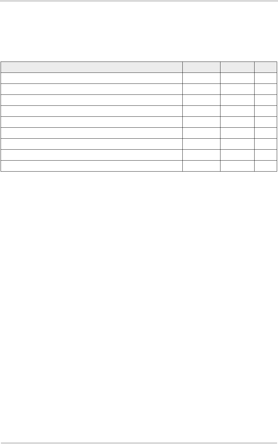
2.1.2.1 Absolute Maximum Ratings
The absolute maximum ratings stated in Table 4 are stress ratings under any conditions.
Stresses beyond any of these limits will cause permanent damage to PLSx3.
Table 4: Absolute maximum ratings
Parameter Min Max Unit
Supply voltage BATT+ (no service) -0.3 +5.5 V
Voltage at all digital pins in POWER DOWN mode -0.3 +0.3 V
Voltage at digital pins 1.8V domain in normal operation -0.2 V180 + 0.2 V
Voltage at SIM interface, CCVCC 1.8V in normal Operation 0 +2.16 V
Voltage at SIM interface, CCVCC 2.85V in normal Operation 0 +3.25 V
Current at SIM interface in 1.8V and 2.85V operation -145 mA
Voltage at ADC pin in normal operation 0.1 +1.7* V
V180 in normal operation +1.7 +1.9 V
USB-Pins -0.3 3.63 V