
Specifications
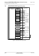
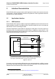
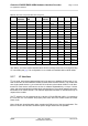
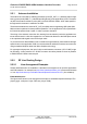
Table Of Contents

Cinterion
®
EHS5-E/EHS5-USR4 Hardware Interface Overview
2.2 RF Antenna Interface
28
ehs5_hio_v04.000 2019-01-16
Confidential / Preliminary
Page 20 of 46
2.2.1 Antenna Installation
The antenna is connected by soldering the antenna pad (RF_OUT, i.e., pad #59) and its neigh-
boring ground pads (GND, i.e., pads #58 and #60) directly to the application’s PCB. The anten-
na pad is the antenna reference point (ARP) for EHS5-E/EHS5-USR4. All RF data specified
throughout this document is related to the ARP.
The distance between the antenna RF_OUT pad (#59) and its neighboring GND pads (#58,
#60) has been optimized for best possible impedance. On the application PCB, special atten-
tion should be paid to these 3 pads, in order to prevent mismatch.
The wiring of the antenna connection line, starting from the antenna pad to the application an-
tenna should result in a 50
line impedance. Line width and distance to the GND plane needs
to be optimized with regard to the PCB’s layer stack.
To prevent receiver desensitization due to interferences generated by fast transients like high
speed clocks on the application PCB, it is recommended to realize the antenna connection line
using embedded Stripline rather than Micro-Stripline technology.
For type approval purposes, the use of a 50
coaxial antenna connector (U.FL-R-SMT) might
be necessary. In this case the U.FL-R-SMT connector should be placed as close as possible
to EHS5-E/EHS5-USR4‘s antenna pad.
2.2.2 RF Line Routing Design
2.2.2.1 Line Arrangement Examples
Several dedicated tools are available to calculate line arrangements for specific applications
and PCB materials - for example from http://www.polarinstruments.com/ (commercial software)
or from http://web.awrcorp.com/Usa/Products/Optional-Products/TX-Line/ (free software).
Embedded Stripline
This figure below shows a line arrangement example for embedded stripline with 65µm FR4
prepreg (type: 1080) and 710µm FR4 core (4-layer PCB).