
Specifications


CINTERION
®
BGS12 Hardware Interface Description
Contents
90 of 109
Page
BGS12 HID_V00.915
Confidential / Released
2019
-
01
-
07
6.2 Mounting BGS12 onto the Application Platform
This section describes how to mount BGS12 onto the PCBs (=printed circuit boards), in-
cluding land pattern and stencil design, board-level characterization, soldering conditions,
durability and mechanical handling. For more information on issues related to SMT module integ-
ration see also [3].
6.2.1 SMT PCB Assembly
6.2.1.1
Land Pattern and Stencil
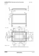
The land pattern and stencil design as shown below is based on Gemalto M2M characterizations
for lead-free solder paste on a four-layer test PCB and a 120 respectively 150 micron thick
stencil.
The land pattern given in Figure 49 reflects the module‘s pad layout, including signal pads and
ground pads (for pad assignment see Section 5.4).
Figure 49: Land pattern (top view)
The stencil design illustrated in Figure 50 and Figure 51 is recommended by Gemalto M2M as
a result of extensive tests with Gemalto M2M Daisy Chain modules.