
Specifications


CINTERION
®
BGS12 Hardware Interface Description
Contents
62 of 109
Page
BGS12 HID_V00.915
Confidential / Released
2019
-
01
-
07
4 Antenna Interface
The RF interface has an impedance of 50Ω. BGS12 is capable of sustaining a total mismatch
at the antenna lines without any damage, even when transmitting at maximum RF power.
The external antenna must be matched properly to achieve best performance regarding radiat-
ed power, modulation accuracy and harmonic suppression. Antenna matching networks are
not included on the BGS12 module and should be placed in the host application if the an-
tenna does not have an impendance of 50Ω.
Regarding the return loss BGS12 provides the following values in the active band:
Table 16: Return loss in the active band
4.1 Antenna Installation
245
1 2 3 4 5 6 7 8 9 10 11 12 13 14 15 16 17 18 19
52 51 50 49 48 47 46 45 44 43 42 41 40 39 38 37 36 35 34
66
65
64
63
62
61
60
59
58
57
56
55
54
53
20
21
22
23
24
25
26
27
28
29
30
31
32
33
67 68 69 70 71 72 73 246
252 74 75 76 77 78 79 80 247
250 100 101 102 103 104 105 106 249
251 93 94 95 96 97 98 99 248
85 86
89 90
87 88
91 92
81 82 83 84
GND
GND
RF_OUT
The antenna is connected by soldering the antenna pad (RF_OUT, i.e., pad #59) and its neigh-
boring ground pads (GND, i.e., pads #58 and #60) directly to the application’s PCB. The an-
tenna pad is the antenna reference point (ARP) for BGS12. All RF data specified throughout
this document is related to the ARP.
Figure 38: Antenna pads (bottom view)
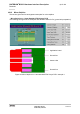
State of
module
Return loss of module Recommended return loss of
application
Receive > 8dB > 12dB
Transmit not applicable > 12dB