
Specifications


CINTERION
®
BGS12 Hardware Interface Description
Contents
38 of 109
Page
BGS12 HID_V00.915
Confidential / Released
2019
-
01
-
07
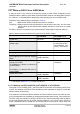
Figure 11: Beginning of power saving if CFUN=7
3.4.6 Power Saving in OFF-state
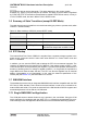
When the BGS12 is powered off, and the BATT
+BB
, BATT
+RF
lines are supplied, the OFF-
current can be lesser than 100uA (V
BATT+
=4.2V). Detail power off state supply current of
I
BATT+
is
shown in Table 27. If the power-off current is a concern, it is suggested to use a
MOSFET as
a switch to reduce the 100uA (V
BATT+
=4.2V) current to the quiescence current of
the MOS-
FET.
The figure below shows an external application circuit that provides the possibility to dis-
connect the module‘s BATT+ lines from the external application‘s power supply. The
MOSFET transistor (T8) should have an RDS_ON value < 50mΩ in order to minimize voltage
drops.
This circuit can also be used to reset the module in case it becomes unresponsive, or to
completely switch off and restart the module after a firmware update.
Afterwards the module can be restarted using the ON signal as described in Section 3.3.1.1.
Figure 12: Power Saving in OFF-state