
Specifications


CINTERION
®
BGS12 Hardware Interface Description
Contents
25 of 109
Page
BGS12 HID_V00.915
Confidential / Released
2019
-
01
-
07
3.2 Power Supply
BGS12 needs to be connected to a power supply at the SMT application interface - 3 lines
each BATT
+BB
, BATT
+RF
and GND. BATT
+BB
is for the general power management and
BATT
+RF
is for the GSM power amplifier supply.
The power supply of BGS12 has to be a single voltage source at BATT
+BB
and BATT
+RF
. It
must be able to provide the peak current during the uplink transmission.
All the key functions for supplying power to the device are handled by the power management
section of the analog controller. This IC provides the following features:
•
Stabilizes the supply voltages for the GSM baseband using low drop linear voltage regulat-
ors and a DC-DC step down switching regulator.
•
Switches the module's power voltages for the power-up and -down procedures.
•
SIM switch to provide SIM power supply.
When power supply is provided on BATT
+BB
and BATT
+RF
pins and BGS12 has not
been powered on, please
make sure to avoid that current is flowing from any other source into the module circuit (for example reverse
current from high state external control lines). The controlling application must be designed to prevent reverse
current flow, otherwise there is the risk of damaging the module.
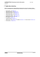
3.2.1 Minimizing Power Losses
When designing the power supply for your application please pay specific attention to power
losses. Ensure that the input voltage V
BATT+
never drops below 3.3V on the BGS12 board, not
even in a GSM transmit burst where current consumption can rise (for peaks values see the
power supply ratings listed in Section 5.5). It should be noted that BGS12 switches off when
exceeding these limits. Any voltage drops that may occur in a transmit burst should not
exceed 400mV.
The module switches off if the minimum battery voltage (V
BattMin
) is reached. Example:
V
BattLowLimit
= 3.3V
D
DropMax
= 0.4V
V
BattMin
= V
BattLowLimit
+ D
DropMax
V
BattMin
= 3.3V + 0.4V = 3.7V
Figure 3: Power supply limits during transmit burst