
Specifications


CINTERION
®
BGS12 Hardware Interface Description
Contents
22 of 109
Page
BGS12 HID_V00.915
Confidential / Released
2019
-
01
-
07
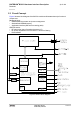
2.3 Circuit Concept
Figure 2 shows a block diagram of the BGS12 module and illustrates the major functional
components:
Baseband block:
•
GSM baseband processor and power management
•
Stacked flash/PSRAM memory
•
Application interface (SMT with connecting pads)
GSM RF section:
•
RF transceiver (part of baseband processor IC)
•
RF power amplifier/front-end module inc. harmonics filtering
•
Receive Balun
Figure 2: BGS12 block diagram