
User`s guide

Award BIOS Description
13
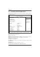
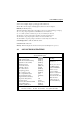
Item Help
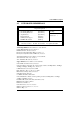
?DRAM Clock/Drive Control
?AGP & P2P Bridge Control
?CPU & PCI Bus Control
Memory Hole
System BIOS Cacheable
Video RAM Cacheable
Delay Prior to Thermal
VGA Share Memory Size
FB Address Conversion
FB Page Close Prediction
[Press Enter]
[Press Enter]
[Press Enter]
[Disabled]
[Disabled]
[Disabled]
[16 Min]
[32M]
[Enabled]
[Enabled]
Menu Level ?
????:Move Enter:Select +/-/PU/PD:Value F10:Save ESC:Exit F1:General Help
F5: Previous Values F6: Fail - Save Defaults F7: Optimized Defaults
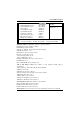
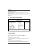
DRAM Clock/Drive Control: Press <Enter> to enter the submenu.
DRAM Clock: By SPD, 100MHz, 133MHz
DRAM Timing: By SPD, Manual.
When choose “Manual”, the following six items will display.
SDRAM CAS Latency: 2, 2.5
Bank Interleave: Disabled, 2 Bank, 4 Bank
Precharge to Active(Trp): 3T, 2T
Active to Precharge(Tras): 6T, 5T
Active to CMD(Trcd): 3T, 2T
DRAM Command Rate:2T Command, 1T Command
DRAM Burst Len: 4, 8
CPU read DRAM Mode: Fast, Medium, Slow
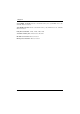
AGP & P2P Bridge Control: Press <Enter> to enter submenu. Default setting is
recommended.
AGP Aperture Size: 64M, 32M, 16M, 8M, 4M, 256M,128M
AGP Mode: 4X, 2X, 1X
AGP Driving Control: Auto, Mnaual
When choose Manual, the following one item can be modified.
AGP Driving Value: DA, 00~FF
AGP Fast Write: Disabled, Enabled
AGP Master 1WS Write: Disabled, Enabled
AGP Master 1 WS Read: Disabled, Enabled
CPU & PCI Bus Control: Press <Enter> to enter submenu
CPU to PCI Write Buffer: Enabled, Disabled
PCI Master 0 WS Write: Enabled, Disabled
PCI Delay Transaction: Disabled, Enabled
Memory Hole Set the memory hole reserved for expanded ISA card. Disabled, 15M-16M