
User's Manual
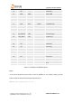
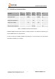
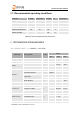
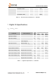
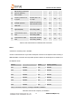
Table Of Contents
- General
- Module introduction
- Hardware description
- Approvals
- CE Approvals (ETSI)
- FCC Approvals
- ATEX Approvals
- Module Pinout
- Hardware Description
- Hardware Diagram
- Interface characteristics
- Absolute Maximum Ratings
- Environmental characteristics
- Recommended operating conditions
- DC Electrical Characteristics
- Digital IO Specifications
- AC Electrical Characteristics
- Physical Dimensions and Footprint
- Physical Dimensions
- Recommended Footprint
- Soldering Temperature Time Profile (for reflow so
- Recommended temperature time profile for lead-fre
- Reliability Test
- Application Precautions
- Safety precautions
- Engineering design and using precautions
- Storage conditions
- Packaging
- Carrier tape
- Reel
- Ordering Information
- Drawing of Product Label
- Disclaimer
- RoHS Declaration
- Data Sheet Status
- Reference Documents
- Contact Information

SZU06A1 Product Manual
SZU06A1 PM(Rev 2.0)
11
5.2 Recommended operating conditions
Parameter
Min value
Typical value
Max value
Unit
Environment
Supply voltage
2.1
3.3
3.9
V
RF input power
-
-
10
dbm
RF frequency
2405
2480
MHz
Operating temperature
-40
25
85
℃
-
Relative humidity
-
-
95
%
Table 5-3 Recommended Operating Conditions
6
DC Electrical Characteristics
V 3.3V,T 25 2400MHz 2483.5MHz.
DD OP C
f ℃,
Parameter
Test condition
Symbol
Value
Min.
Type
Max.
Supply Voltage
V
D D
2.1V
3.3V
3.9V
Supply Current
I
VDD
-
-
1000mA
Reset
I
reset
2.1mA
3mA
Hard reset
r e s e t
t
1ms
FLASH
FLSH erase
C
era se
10000
-
-
Flash data retention
t
r e te n ti o n
10years
-
-
Page erase
t
era se
20ms
40ms
I
r e a d
-
-
3mA
Write operation
I
w rit e
-
-
3mA
RX Current
Receive enable
I
R X
-
13.7mA
14.2mA
TX Current
TX power = 0dBm
I
TX
-
15mA
16.7mA
TX power = 3dBm
-
20.2mA
21mA
TX power = 8dBm
-
29.7mA
31mA
Sleep Current
Enter EM2 mode
I
sleep
2.2μA
2.7μA
3.2μA
Enter EM3 mode
-
1.7μA
-
Enter EM4 mode
-
0.5μA
-
Wake up time
From EM1 to wake
1
t
em w u
-
3μs
-