(without price) SF-8500(LX-575) AUG.
CONTENTS 1. SCHEMATIC DIAGRAM................................................................................................ 1 2. SPECIFICATIONS ......................................................................................................... 5 3. TO REPLACE THE BATTERY ...................................................................................... 6 4. ERROR MESSAGE ....................................................................................................... 7 5.
1. SCHEMATIC DIAGRAM 1-1.
1-2.
1-3.
2.
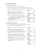
3. TO REPLACE THE BATTERY A) To replace the main batteries Before replacing the main batteries, note the following precautions. • Do not remove the back-up battery from the SF Unit while main batteries are removed. • Be sure to replace both batteries at the same time, and do not use an old battery with a new one. 1. Remove the screw that hold the battery compartment cover in place. 2. Remove the battery compartment cover by sliding it in the direction indicated by the arrow in the illustration. 3.
4. ERROR MESSAGE Message Meaning Action Text specified for search does not exist. Correct or change specified text. Wrong password entered. Enter correct password. MEMORY FULL! No more room in memory for storage of data. Delete unnecessary data items from memory. DATA ERROR! CONSULT YOUR OWNER'S MANUAL UNDER "DATA ERROR" Abnormal data caused by strong impact, static electricity, etc. Consult the "DATA ERROR" section on page 2 of owner's manual. DATA ITEM NOT FOUND! PASSWORD MISMATCH! 5.
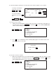
Following the RESET operation, the Home Time Display appears. The initial settings of the SF Unit after reset are shown below. HOME TIME: Washington D.C. JAN/1/1994 (SAT) 12:00 AM 12-hour format WORLD TIME: New York Daily Alarm: 12:00 PM Sound: Schedule alarm Daily alarm Key Character input: CAPS 6. ON OFF ON TO SAVE THE DATA TO OTHER MACHINE SF-8500 can transfer customers data to other SF-8500 with memory protection only when replacing the LCD or the outer case. How to transfer the data.
4) Check the hardware parameters, and if the units have another condition, reset as follows. To change the hardware parameters, press the , , and cursol keys. To set the hardware parameters, press the set key. *** HARDWARE PARAMETERS PARITY BIT LENGTH7 bits BPS 1200 EVEN 2400 *** ODD 7 bits 4800 NONE 8 bits 9600 TEL TEL FUNCTION 4 4 5) Set up the slave machine.
2 Press 1 to select "TRANSMIT" and the following menu appears. 1 ONE DATA ITEM 2 MODE DATA ITEMS 3 ALL DATA ITEMS 1 — SEND — TEL 3 Press 3 to select "ALL DATA ITEMS", and the following display appears to confirm whether you wish to proceed. SEND ALL DATA ITEMS ? 3 YES SET / NO ESC TEL 4 Press the SET key to proceed with the data transmission, or press ESC if you wish to cancel.
Message Cause STOPPED ! 7. • ESC key pressed on transmitting or receiving unit. • Memory area of receiving unit full. • Battery power drops below a certain level. TRANSMIT ERROR ! Cable connection broken or abnormal noise in cable. MEMORY FULL ! Memory area of receiving unit full. TO CHECK THE MEMORY CAPACITY There are two types of Memory Capacity Display, as shown below: SF UNIT: Total memory used for storage of Telephone Directory, Business Card Library, Memo, Calendar, and Schedule Keeper data.
8. DISASSEMBLY (SF-8500) 1) To open display unit 1. Remove the key switch sheet from the display frame with care using a sharp tweezers and remove 2 screws, then remove the display back cover. 2. Remove the blind plate of hinge and then release the 2 screws of hinge cover. 3. Release the 5 screws of display PCB and remove the display PCB.
2) To open battery cover and back cover 1. Release the one screw of battery cover and remove the battery cover. 2. Remove the batteries. (Refer section 3 in this manual.) 3. Release the 8 screws of the back cover. Then, remove the back cover. 4. To check the circuit by oscilloscope, apply the power to main PCB as follow: External Power supply Switch GND Prepare some 2P switch for Main switch. +6V +3V Prepare some power supply for + 6V and +3V.
9.
10. CIRCUIT EXPLANATIONS 10-1. System chart Generally, SF-8500 is working with the following steps.
10-2. Power supply circuit 1) Power supply circuit for CPU, GATE ARRAY, CG ROM and RAMs. When the memory back-up battery or main batteries are set, the voltage supplies at the terminal VDD1 (Pin No.1) of SC371015FU (LSI2) through the diode MA743 (D1). When LSI2 receives a voltage, the regulated voltage VDD (4.3V~4.7V) will be applied to the VDD lines from the terminal VO1 (Pin No.2). HD62076C02 (LSI1), µPD65005GC-566 (LSI3), HD62063B01 (LSI4), and M5M51008AFP-10LL (LSI5) are connected the VDD lines.
When the voltage from the main batteries becomes +3.7V ±0.1V, the terminal VCOMP0 (Pin No.5) of the power supply chip (LSI2) becomes "L" level, then this signal goes to the terminal PDN (Pin No.28) of the GATE ARRAY (LSI3). After this, the terminal VOT (Pin No.32) of GATE ARRAY (LSI3) become "L" level, and the terminal PDB (Pin No. 31) of the power supply chip (LSI2) receives this signal. In this condition, the voltages for LCD will be cut off compulsorily.
7) Power supply chip SC371015FU + The IC SC371015FU is power supply chip for SF-8500. When IC SC371015FU receives a Voltage 5V from main power supply circuit at the terminal VDD1(Pin No.2), the regulated voltage VDD (4.3~4.7V) will be applied to the VDD lines. The outputs VSS (VREG) and V1~V4 are the LCD drive voltages. When the terminal PDB becomes "H", those voltages are generated by IC SC371015FU and capacitors C3 and applied to LCD driver IC MSM6385AV-Z-358B.
8) Gate array GND Open (Pin 26) TO MAIN SWITCH "L" (Pin 40) (Pin 25) LSI SWO MON GATE ARRAY µPD65005GC-566-3B6 "H" TO CPU INT0 terminal (Pin 70) 9) (Pin 27) LSO (Pin 34) (Pin 7) (Pin 33) VDD GND CSB (Pin 24) "H" FROM CPU CS2 terminal (Pin 28) When VDD is applied from power supply IC SC371015FU to gate array µPD65005GC-5563B6, gate array will send "L" signal to active the main switch signal from terminal SWO.
10) Power supply for LCD (Pin69) (Pin32) "H" (Pin31) PDB VOT INT1 CPU V2ON "H" (Pin45) (Pin31) HD62076C02 VIN GATE ARRAY µPD65005GC-566-3B6 POWER SUPPLY CHIP SC371015FU LCD drive voltages VREG,V1~V4 When the system is start up, CPU will send "H" signal to VIN terminal of gate array from V2ON terminal. Then, gate array will send "H" signal from VOT terminal to release interruption signal INT1 of CPU and also, it will be sent to PDB terminal of power supply chip to generate LCD drive voltages.
10-3. CPU pin description (HD62076C02) Pin No.
10-4. Gate array pin descriptions (µPD65005GC-566-3B6) Pin No. Name In/Out Status of OFF Status of ON Description 1~6, 8, 9 7, 33 10 11~13 14 15 16~23 24 25 26 27 28 29 30 31 32 34 35 36 37 38 39 40 41 42 43 44 45, 51 46, 47 48 49 50 52 OI7~OI0 GND B15 A15,A01,A00 N.C.
Pin No.
10-7. Operation program ROM pin discriptions (µPD23C4001EBGW-304) Pin No. Name In/Out Status of OFF Status of ON Description 2~12,23, 25~31 13~15, 17~21 16 22 24 1, 32 A0~A18 In L Pulse Address bus line (A0~A14, RA15~RA18) O0~O7 GND CEB OEB N.C., VCC Out In In In In L L H L L Pulse L Pulse Pulse H Data bus line (IO0~IO7) GND terminal Chip enable signal from Gate array Output enable signal from Gate array VDD terminal 10-8. RAM pin discriptions (M5M51008AFP-10LL) Pin No.
11. DIAGNOSTIC OPERATION Main switch Check pad 1. Diagnostic mode SELECT MENU 1 DISPLAY 2 MEMORY 3 KEY 4 BUZZER 5 I/F The diagnostic mode appears when main switch is turned on while there is a short in the checkpad. After this operation, the machine will beep and display "SELF-TEST". The menu appears after press SET key. Tests are conducted by selecting the mode from the list on screen. The each test can be selected by the following function keys.
3. ROM/RAM check DISP CHNG key MEMORY INT #1 1 WRITE 2 READ 3 CHKSUM 4 SPECIFIC 5 RTC SPREADSHEET key TEL key BUSINESS CARD key INT---Internal RAM EXT--External RAM(RAM card) #1---Test data pattern(00,01,02...) #2---Test data pattern(FF,FE,FD....) MEMO key SCHEDULE key :Return to menu : Write the set pattern to the selected RAM area : Compare the pattern displayed after # with the write data of RAM and displays the results. : Dump contents of memory.
3) CHECK SUM When memory dump is operated by pressing BUSINESS CARD button, a display will appear as shown at left. The first two lines, begining from the top left, signify the following address values in reference to the one megabyte "E0" area: 00001,00002,00004,....,00080,00100,00200 00400,00800,01000,....,20000,40000,80000 The lower two lines refer to the data in the "E1" area. TYPE SIZE CHECK-SUM XOR E0 ROM 512KB 342B 6D CE RAM 128KB 8300 00 Type : ROM and RAM are shown.
5. Buzzer check BUZZER 1 BEEP 2 ALARM 1 3 ALARM 2 EXECUTING ! SPREADSHEET key : Key input sound every 1 second TEL key : Sound alarm 1 BUSINESS CARD key : Sound alarm 2 Sound can be stopped by pressing the any key. While an alarm is sounding the screen display is as shown at left. If an irregularity is found in voltage of battery while the alarm is sounding, the alarm will stop. After 256 seconds, the alarm will stop automatically. 6.
NOTE : As diagnostic program area does not have all ASCII code, to display a reception data, some charactor will be changed to other charactor. For example, a chapital letter will be changed to small letter. Break display (Broken transmission) Error display TRNS ERROR ! TRNS BREAK ! 7. Battery level check Memory back up battery The memory back up voltage detector detects any irregularity in voltage, the machine goes into an error state and the display is as shown at left figure.
12. TROUBLESHOOTING Generally, check the machine with the followning steps for repair. CONDITION : Main battery switch ON START No Main battries 6V? Yes Replace main battries (CR2032 2pcs.) (Clean and adjust battery contact.) 1 Key input OK? Yes No Reset operation No Display OK? Yes Yes Save data to P/C if necessary. Key input OK? No Current consumption OK? No Yes Follow repair section 2. Load data from P/C if necessary. Follow repair section 1. No Data OK? Yes Follow repair section 3.
2 Connection of keyboard cable OK? Yes No No When press power on Key, any oscillation at oscillator? 1 Adjust keyboard cable. Poor connection Yes on oscillator? Yes Solder line No 1 Replace parts. No Pin 45 of HD62076C02 "H" ? Poor connection? No Yes Yes Solder line 1 Replace parts. Pin 31 of µPD65005G-566-3B6 "H" ? Yes Pin 32 of µPD65005G-566-3B6 "H" ? Yes No Solder line No Poor connection? Yes Solder line No 1 Replace parts.
Repair section 2 : For no display or wrong display problem START Pin 32 of µPD65005G-566-3B6 "H" ? No Poor connection? No Yes Yes Solder line 1 Replace parts. No Solder line Pin 31 of SC371015FU "H"? Yes LCD drive voltages OK? (Pin8~12) of Yes SC371015FU No Poor connection? No 1 Yes Poor connection on chip Yes resistors R8~R10 ? No Yes Poor connection on capacitor C7~C8 ? No Chip capacitor OK ? Yes Chip resistor OK? Yes Solder line No No Replace parts. Replace SC371015FU.
13.
— 34 —
14.
15.
8-11-10, Nishi-Shinjuku Shinjuku-ku, Tokyo 160, Japan Telephone: 03-3347-4926