
User guide


S1A0071 Audio Processor for Class-D Power AMP
Digital & Analog Co., Ltd. (Rev. 1.0) -5-
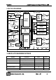
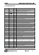
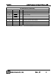
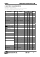
4. PIN DESCRIPTION
NO. Name I/O Description
1 OPT I
Active high. If it is high, PWM output is activated after power
ON Mute Time, T
M
. Otherwise (Default = HIGH)
2 OSCEN I Triangle wave generator enable input
3 SIO B Triangle wave I/O
4
MUΤΕ
I Mute control input. It is also used for external protection.
Active low. Low state is muted state.
5 VD O Logic power supply pin (internal generated)
6,7,8,9 CX_L B L-channel amp capacitor connected pin for Phase & gain
10 VO_L O L-channel pre-amp output pin for gain setting
11 VIN_L I L-channel pre-amp input pin
12 GND_A P L-channel sound ground
13 GND_A P R-channel sound ground
14 VIN_R I R-channel pre-amp input pin
15 VO_R O R-channel pre-amp output pin for gain setting
16,17,18,19 CX_R B R-channel amp capacitor connected pin for Phase & gain
20 PDCTR I P-MOS gate delay setting pin
21 NDCTR I N-MOS gate delay setting pin
22 VB O Regulated voltage output pin for internal current bias
23 VC I Triangle wave magnitude setting input
24 CDLY I Time delay capacitor pin for internal use
25 VSS P Negative power supply pin
26 VLN I Soft clipping low level input
27 CF2_R I R-channel current feed back input 2
28 CF1_R I R-channel current feed back input 1
29 VF_R I R-channel voltage feed back input
30 GND_CH P Control block ground
31 GND_A P Reference block ground
32 PDSENS I Power Down Detection
33 VPSENS I The operating voltage detection pin of the external
MOSFET. When its function is not used, this pin must be
tied to VCC and about 0.1uF is connected to GND
34 NO_R O R-channel N-MOS switching output (PWM)
35 PO_R O R-channel P-MOS switching output (PWM)
36 NS3 - NC (Test pin for evaluation)
37 NS2 - NC (Test pin for evaluation)
38 PO_L O L-channel P-MOS switching output (PWM)
39 NO_L O L-channel N-MOS switching output (PWM)