
User guide

S1A0071 Audio Processor for Class-D Power AMP
Digital & Analog Co., Ltd. (Rev. 1.0) -18-
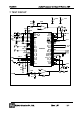
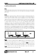
Note 7
When power is turned on, the circuit operates unstably, possibly generating noise. To prevent
this unstable situation, the S1A0071 use the CDLY pin (pin# 24), which can be connected to a
capacitor. This CDLY pin used to generate a slight time delay from power up to when the
circuit starts to operate normally. The CDLY pin drive’s capacity is about 1.0㎂ and the mute
mode sustains until the externally connected capacitor charges to a voltage equal about VB
(pin 22). The time delay can be calculated as follows:
CETa
C
Ta
I
CVC
Tdly ×≅+
×
=+
×
= 60.3
0.1
3
(sec)
μ
(Ta « Tdly)
T
a
is the internal processing time that used in the removal of circuit settling time and other
pop noises. Tdly also decides the protection restart time. Among the protection functions in
S1A0071, those that remove "causes" (Thermal Protection, Over Current Protection) oscillate
from normal operation → protection → normal operation → protection → … , generating
very fast blocking oscillation. The Tdly decides (delays) the repeat cycle of the oscillation,
which protects the circuit and controls unstable operations. Those protection functions
(Output DC Short) that do not remove "causes" are not affected by Tdly, and once the cause
has been removed, they return to normal operation.
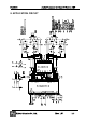
Note 8
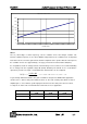
S1A0071 has a built-in limiting block at the input stage that remove noise signal that may be
generated by discontinuous feedback and also this limit block operate as a clipping circuit due
to over-input signal. When a specific voltage (± Vls) is applied to VLP and VLN, the soft
clipping function starts to operate on the input whose value lie outside the ± Vls range, on the
basis of the Pre Amp output with its gain set by R1 and R2. As a result, the entire circuit is
enabled to drive only the signals that lie within the operating range, thus maintaining a
continuous feedback loop which allows the circuit to output a soft clipped output waveform
even for an input lying outside the output dynamic range.
Vls must be set differently according to the MOSFET power supply voltage and power supply
impedance, and MOSFET ON resistance. If we assume that the power supply impedance is
ideal (= 0) and MOSFET ON resistor is ideal (0 Ohm), the appropriate values for Vls values on
the power supply voltage (VCCP, VSSP) would be as follows:
VCCP, VSSP
± 20V ± 30V ± 45V
Vls
± 1.05V ± 1.43V ± 2.15V