
Instruction Manual
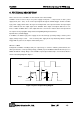

S1A0051 FET Driver for Class-D PWM Amp
Digital & Analog Co., Ltd. (Rev. 1.0) -4-
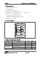
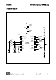
4. PIN DESCRIPTION
NO. Name I/O Description
1 VCC P Positive power supply pin
2 NC - No Connected
3 VI1 I Logic Driver Input 1
4 VI2 I Logic Driver Input 2
5 VI3 I Logic Driver Input 3
6 VI4 I Logic Driver Input 4
7 NC - No Connected
8 VSS P Negative power supply pin
9 VCC34 P Positive power supply pin for driver 3, 4
10 VO4 O Logic Driver Output 4
11 VO3 O Logic Driver Output 3
12 VSS34 P Negative power supply pin for driver 3, 4
13 VSS12 P Negative power supply pin for driver 1, 2
14 VO2 O Logic Driver Output 2
15 VO1 O Logic Driver Output 1
16 VCC12 P Positive power supply pin for driver 1, 2
* I: Input, O: Output, B: Bi-directional, P: Power Supply, -: No Connection.
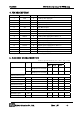
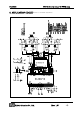
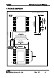
5. ELECTRIC CHARATERISTICS
With no special mentions, Ta = 25°C, VCC = 10V
Characteristic Symbol Condition Value Unit
Min. Typ. Max.
Supply Current ICC1 VCC = 10V
All input pin is Low State
1 3 5 mA
ICC2 VCC = 12V
All input pin is Low State
1.5 3.7 6.0 mA
Switching Characteristics
Output Rising Time Tr CL=1nF - 15 80 nsec
Output Falling Time Tf CL=1nF - 15 80 nsec
Propagation Delay Td CL=1nF - 20 50 nsec
Driving Characteristics
Output High Level VOH Ipull = 5mA 9.0 9.25 9.5 V
Output Low Level VOL Ipush = 5mA - - 0.4 V
Input Threshold
High State Logic 1 VIH - 3.3 - - V
Low State Logic 0 VIL - - - 0.5 V