
User's Manual


5.6
Fault Finding
M889-00
02/10/95 Copyright TEL
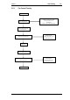
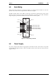
T889 PCB Layout
Bottom Side
L46
C97 C98
L19
L29
L96
C59
L22 L16
L32 L26
L1
L49 L43L12
L39 L33
C45
C38
C15
C32
C25
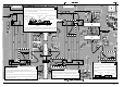
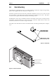
Output Test Lead - Q1 & Q2
1. Desolder C15 and resolder on edge as shown.
2. Remove the wireline clamping plate and solder the test lead outer core to the outer
core of the wireline (L14 shown).
3. Solder the inner core of the test lead to the raised end of C15.
4. To test Q1 & Q2, provide 2.5-3W drive power to Q1 through the input test lead. While
testing, ensure that the output test lead on Q2 is terminated at all times into a good
50
Ω
RF load.
main PCB
Teflon PCB
L14
L12
C15 (DC blocking capacitor)
output test lead
(transmission line)
(wireline)
(to wattmeter, analyser etc.)
50
Ω
test point
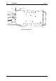
Input Test Lead - Q1 & Q2
1. Desolder the inner core of L1 and lift off its pad.
2. Solder the test lead outer core to the earth plane (remove
the resist first).
3. Solder the inner cores of L1 and the test lead together off
the PCB.
main PCB
L1
input test lead
50
Ω
test point
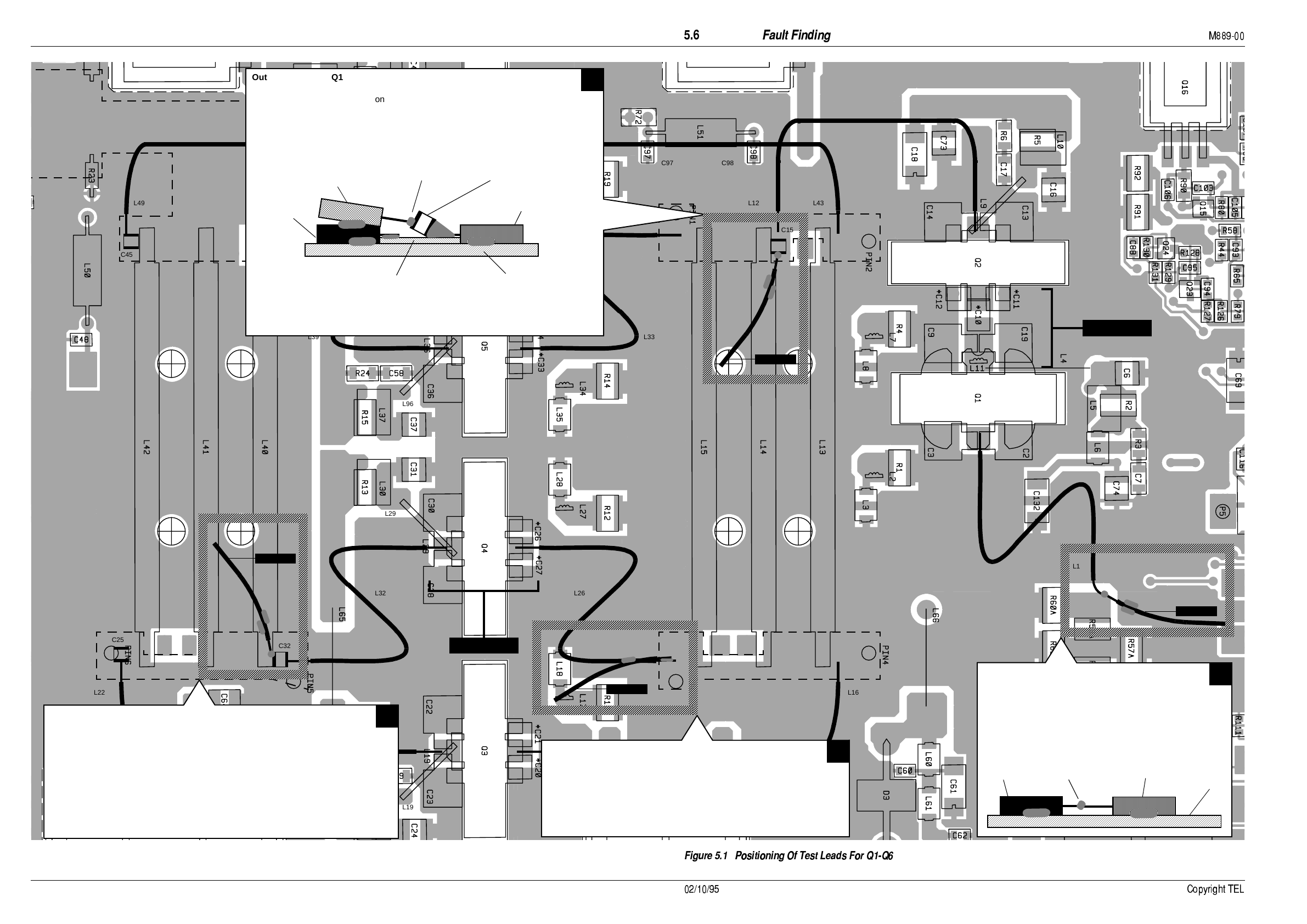
Output Test Lead - Q3-Q6 (Q4 Shown)
Refer to drawing B above.
1. Desolder the appropriate DC blocking capacitor and resolder on edge.
2. Remove the wireline clamping plate and solder the test lead outer core to the outer
core of the wireline.
3. Solder the inner core of the test lead to the raised end of the DC blocking capacitor.
4. To test, drive the transistor with approx. 10W over the range 800-870MHz and expect
a minimum output of 30W.
Input Test Lead - Q3-Q6 (Q4 Shown)
1. Desolder the appropriate transmission line inner core and lift off its pad.
2. Solder the test lead outer core to the transmission line outer core.
3. Solder the inner cores of the transmission line and test lead together off
the PCB.
not 50
Ω
not 50
Ω
test lead
test lead
test lead
test lead
A
B
C
D
Figure 5.1 Positioning Of Test Leads For Q1-Q6