
User's Manual
M889-00
Circuit Operation 2.3
Copyright TEL 02/10/95
2.1 Introduction
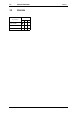
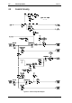
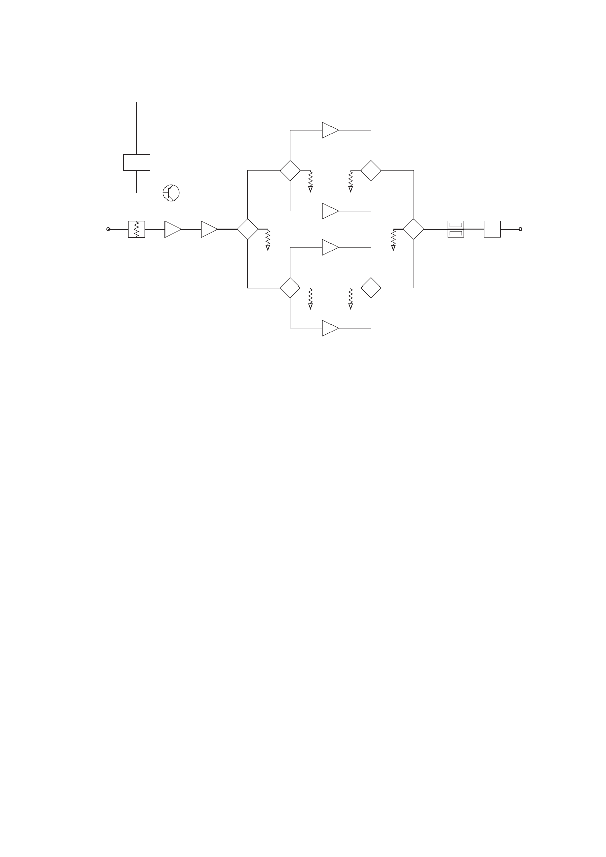
Figure 2.1 High Level Block Diagram
The T889 comprises a three stage RF power amplifier with extensive control circuitry.
The final stage is composed of four transistors (Q3, Q4, Q5 & Q6) whose outputs are
combined to provide the rated output power.
The configuration of each of the main circuit blocks may be seen on a functional level in
Figure 2.1.
2.2 RF Circuitry
The driver stage of the T889 consists of a two stage transistor amplifier (Q1, Q2) which
delivers a minimum of 40W. This signal is split via three 3dB couplers (L13, L14 & L15)
and used to drive the four final amplifiers (Q3, Q4, Q5 & Q6). These outputs are recom-
bined by L40, L41 & L42 and passed to the antenna socket via the directional coupler
and low pass filter.
The directional coupler senses forward and reflected power, which is rectified (D1, D2)
and passed to the control circuitry for metering, alarm and power control purposes.
Power control is via a series pass transistor (Q16), which controls the supply voltage on
the collector of the driver transistor (Q1).
RF Out
Q1 Q2
Pad
RF In
LPF
4W 40W
Q3
Q4
Q5
Q6
30W
30W
30W
30W
60W
60W
120W
100W
Power
Control
Vsupply
Q16
L40L13
L15 L42
L14 L41
Directional
Coupler