
User Manual


CIRCUIT DESCRIPTION
4-8
June 1997
Part No. 001-3492-001
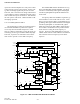
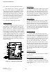
Q130, Q131 and Q132 act as switches that turn
on with the RX_EN line. When J201, pin 4 goes low,
Q130 is turned off, which turns on Q131 that turns on
Q132. This applies +13.3V to U130 before the
TX_EN line on J201, pin 3 goes high.
U130B provides the key-up/key-down condition-
ing circuit. C141/R137 provide a ramp up/ramp down
of the +9V TX during key-up/key-down which
reduces load pull of the VCO during key-up.
The output on U130B, pin 7 is applied to the non-
inverting input of comparator U130D, pin 12. The
output of U130D, pin 14 is applied to the base of cur-
rent source Q135. The output of Q135 is on the emit-
ter and is applied back to the inverting input of com-
parator U130D, pin 13. A decrease or increase at
U130D, pin 13 causes a correction by U130D to stabi-
lize the +9V transmit output. R140/R141 establishes
the reference voltage on U130D, pin 13. C144 pro-
vides RF bypass, C143 provides RF decoupling and
C145 stabilizes the output. The +9V transmit voltage
is then distributed to the circuits.
4.5 VOLTAGE REGULATORS
4.5.1 +9.6 AND +5.5V REGULATED
The +3-16V applied on J201, pin 5 is applied to
the base of Q110 turning the transistor on. This
causes the collector to go low and applies a low to the
control line of U110, pin 2 and R110 provides supply
voltage isolation. The +13.3V from J201, pin 2 is on
U110, pin 6 to produce a +5.5V reference output on
U110, pin 4. C110 stabilizes the voltage and C114/
C111 provide RF decoupling. C117 provides RF
bypass and C123 provides RF decoupling. C119
helps to stabilize the voltage when the +5.5V supply
first turned on.
The low from the collector of Q110 is also
applied to the control line of U111, pin 2. The +13.3V
from J201, pin 2 is on U111, pin 6 to produce a +9.6V
output on U111, pin 4. C118 provides RF bypass and
C122 provides RF decoupling. C120 helps to stabilize
the voltage when the +9.6V supply first turned on.