
User Manual


CIRCUIT DESCRIPTION
4-7
June 1997
Part No. 001-3492-001
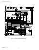
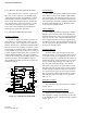
4.4 TRANSMITTER CIRCUIT DESCRIPTION
4.4.1 DRIVER
The VCO RF output signal is applied to R846,
R847 and R848 that form a resistive splitter for the
receive first local oscillator and the transmitter. The
VCO signal is then applied to a 50 ohm pad formed by
R500, R501, and R502. This pad provides attenuation
and isolation. Q500 provides amplification and addi-
tional isolation between the VCO and transmitter.
Biasing for this stage is provided by R503 and R504,
and decoupling of RF signals is provided by C504.
Impedance matching to the power amplifier is pro-
vided by L500/C505.
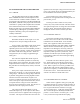
4.4.2 FINAL, COMPARATOR
RF module U510 has an RF output of 1 to 5W
and operates on an input voltage from 10-16V.
Power control is provided by U520, U130, Q520
and a stripline directional coupler. The power is
adjusted by Power Set Control of U900 that provides a
reference voltage to U130C. U130C drives Q520 and
PA module U510 when using the DAC. When not
using the DAC, the set voltage is applied through
U902, pin 2.
One end of the stripline directional coupler is
connected to a forward RF peak detector formed by
R535, CR530, C531 and U520A. The other end of the
stripline directional coupler is connected to a reverse
RF peak detector formed by R537, CR531, C534 and
U520B.
If the power output of U510 decreases due to
temperature variations, etc., the forward peak detector
voltage drops. This detector voltage drop is buffered
by U520A and applied to inverting amplifier U130C
which increases the forward bias on Q520. The
increase on Q520 increases the power output level of
U510. If the power output of U510 increases, the for-
ward peak detector voltage increases and U130C
decreases the forward bias on Q520. The decrease on
Q520 decreases the output power of U510.
The output of CR530 and CR531 are fed to
U520A/B respectively. If the output of either buffer
increases, the increase is applied to the inverting input
of U130C. The output of U130C then decreases and
Q520 decreases the input voltage to U510 to lower the
power. The control voltage is isolated from RF by fer-
rite bead EP510 and C511 decouples RF.
The forward/reverse power voltages from
U520A/B are also applied to U901 for Diagnostic out-
puts on J201, pin 14.
The low-pass filter consists of C541, L540,
C542, L541, C543, L542 and C544. The filter attenu-
ates spurious frequencies occurring above the transmit
frequency band. The transmit signal is then fed
through the antenna switch to antenna jack J501.
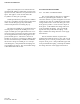
4.4.3 ANTENNA SWITCH
The antenna switching circuit switches the
antenna to the receiver in the receive mode and the
transmitter in the transmit mode. In the transmit
mode, +9V is applied to L543 and current flows
through diode CR540, L544, diode CR541, and R540.
When a diode is forward biased, it presents a low
impedance to the RF signal; conversely, when it is
reverse biased (or not conducting), it presents a high
impedance (small capacitance). Therefore, when
CR540 is forward biased, the transmit signal has a
low-impedance path to the antenna through coupling
capacitor C546.
L544 and C552 form a discrete quarter- wave
line. When CR541 is forward biased, this quarter-
wave line is effectively AC grounded on one end by
C552. When a quarter-wave line is grounded on one
end, the other end presents a high impedance to the
quarter-wave frequency. This blocks the transmit sig-
nal from the receiver. C545/C546 matches the
antenna to 50 ohms in transmit and receive.
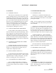
4.4.4 TRANSMIT KEY-UP CONTROL
When 3-16V is applied to J201, pin 3 (TX_EN)
is applied to the base of Q133 it turns the transistor on
and causes the collector to go low. This low is on the
base of Q134 and turns the transistor on to apply
+5.5V to U130A, pin 2. C130 and C131 decouple RF.
The +5.5V from Q134 is divided by R132/R133 to
produce a +3.6V reference on U130A, pin 3. C136,
C137, C138 and C139 provide RF decoupling.