
User Manual


CIRCUIT DESCRIPTION
4-5
June 1997
Part No. 001-3492-001
4.2.7 SYNTHESIZER INTEGRATED CIRCUIT
(U800)
Introduction
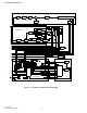
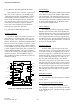
Synthesizer chip U800 is shown in Figure 4-2.
This device contains the following circuits: R (refer-
ence), Fractional-N, NM1, NM2 and NM3; phase and
lock detectors, prescaler and counter programming
circuitry. The basic operation was described in Sec-
tion 4.2.1.
Channel Programming
Frequencies are selected by programming the R,
Fractional-N, NM1, NM2 and NM3 in U800 to divide
by a certain number. These counters are programmed
by Loader board or a user supplied programming cir-
cuit. More information on programming is located in
Section 3.
As previously stated, the counter divide numbers
are chosen so that when the VCO is oscillating on the
correct frequency, the VCO-derived input to the phase
detector is the same frequency as the reference oscilla-
tor-derived frequency.
The VCO frequency is divided by the internal
prescaler and the main divider to produce the input to
the phase detector.
4.2.8 LOCK DETECT
When the synthesizer is locked on frequency, the
SYNTH LOCK output of U800, pin 18 (J201, pin 7) is
3V. When the synthesizer is unlocked, the output is a
less than 1V. Lock is defined as a phase difference of
less than 1 cycle of the TCXO.
4.3 RECEIVER CIRCUIT DESCRIPTION
4.3.1 CERAMIC FILTER, RF AMPLIFIER
Capacitor C200 couples the receive signal from
the antenna switch to ceramic filter Z200. (The
antenna switch is described in Section 4.4.3.) Z200 is
a bandpass filter that passes only a narrow band of fre-
quencies to the receiver. This attenuates the image
and other unwanted frequencies.
Impedance matching between the Z200 and RF
amplifier Q201 is provided by C201, C203 and L200.
CR200 protects the base-emitter junction of Q201
from excessive negative voltages that may occur dur-
ing high signal conditions. Q200 is a switched con-
stant current source which provides a base bias for
Q201. Q200 base bias is provided by R200/R201.
Current flows through R202 so that the voltage across
it equals the voltage across R200 (minus the base/
emitter drop of Q200). In the transmit mode the
receive +9.6V is removed and Q200 is off. This
removes the bias from Q201 and disables the RF
amplifier in transmit mode. This prevents noise and
RF from being amplified by Q201 and fed back on the
first injection line.
Additional filtering of the receive signal is pro-
vided by Z201. L201 and C206 provide impedance
matching between Q201 and Z201. Resistor R205 is
used to lower the Q of L201 to make it less frequency
selective.
4.3.2 MIXER
First mixer Q211 mixes the receive frequency
with the first injection frequency to produce the
87.85 MHz first IF. Since low-side injection is used,
the injection frequency is 87.85 MHz below the
receive frequency. The RF signal is coupled to the
mixer through C211. L212 and C214 tune the mixer
output to 87.85. R214 lowers the Q of L212.
4.3.3 FIRST LO AMPLIFIER
The first injection frequency from the VCO is
coupled to the First Local Oscillator (LO) amplifier
Q260/Q261 through C266. L261/C265 match Q260
to the VCO.
Q261 is a switched constant current source which
provides a base bias for Q260. Q261 base bias is pro-
vided by R264/R265. Current flows through R263 so
that the voltage across it equals the voltage across
R264 (minus the base/emitter drop of Q261). In the
transmit mode the receive +9.6V is removed and
Q261 is off. This removes the bias from Q260 and
disables the First LO amplifier in transmit mode.