
User Manual


CIRCUIT DESCRIPTION
4-3
June 1997
Part No. 001-3492-001
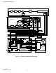
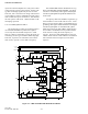
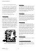
4.2.1 VOLTAGE-CONTROLLED OSCILLATOR
Oscillator
The VCO is formed by Q820, several capacitors
and varactor diodes, and ceramic resonator L826. It
oscillates at the transmit frequency in transmit mode
and first injection frequency in the receive mode (928-
960 MHz in transmit and 840.150-872.150 MHz in
receive).
Biasing of Q820 is provided by R823, R824 and
R826. An AC voltage divider formed by C844 and
C845 initiates and maintains oscillation and also
matches Q820 to the tank circuit. Resonator L826 is
grounded at one end to provide shunt inductance to
the tank circuit.
Frequency Control and Modulation
The VCO frequency is controlled by a DC volt-
age across varactor diode CR824. As voltage across a
reverse-biased varactor diode increases, its capaci-
tance decreases. The VCO frequency increases as the
control voltage increases. The control line is isolated
from tank circuit RF by choke L825. The amount of
frequency change produced by CR824 is controlled by
series capacitor C836.
The VCO frequency is modulated with the trans-
mit audio/data signal from J201, pin 6 is applied
across varactor diode CR822 which varies the VCO
frequency at an audio rate. Series capacitors C825/
C824 couple the VCO to CR822. R821 provides a
DC ground on the anodes of CR822/CR823, and isola-
tion is provided by R820 and C826. C827 is an RF
bypass.
The DC voltage across CR823 provides compen-
sation to keep modulation relatively flat over the
entire bandwidth of the VCO. This compensation is
required because modulation tends to increase as the
VCO frequency gets higher (capacitance of CR824/
CR825/CR826/CR827 gets lower). CR823 also bal-
ances the modulation signals applied to the VCO and
TCXO. The DAC can be used to adjust the VCO
modulation sensitivity.
The DC voltage applied across CR823 comes
from the modulation adjust control R818 on the RF
board. R820 applies a DC biasing voltage to CR822;
C815 provides DC blocking. RF isolation is provided
by C827, R822 and R817.
4.2.2 VCO AND REFERENCE OSCILLATOR
MODULATION
Both the VCO and reference oscillator (TCXO)
are modulated in order to achieve a flat frequency
response. If only the VCO were modulated, the phase
detector in U800 would sense the frequency change
and increase or decrease the VCO control voltage to
counteract the change (especially at the lower audio
frequencies). If only the reference oscillator fre-
quency is modulated, the VCO frequency would not
change fast enough (especially at the higher audio fre-
quencies). Modulating both VCO and reference oscil-
lators produces a flat audio response. Potentiometer
R818 sets the VCO modulation sensitivity so that it is
equal to the reference oscillator modulation
sensitivity.
4.2.3 CASCADE AMPLIFIERS
The output signal on the collector of Q820 is cou-
pled by C846 to buffer amplifier Q821/Q822. This is
a cascade amplifier which provides amplification and
also isolation between the VCO and the stages which
follow. The signal is capacitively coupled from the
collector of Q822 to the base of Q821. The resistors
in this circuit provide biasing and stabilization, and
C852 and C854 are RF bypass capacitors.
4.2.4 AMPLIFIER
Amplifier Q823 provides amplification and isola-
tion between the VCO, Receiver and Transmitter.
C851 provides matching between the amplifiers. Bias
for Q823 is provided by R840, R842 and R843.
Inductor L833 and capacitor C860 provide impedance
matching on the output.
4.2.5 VOLTAGE FILTER
Q845 on the RF board is a capacitance multiplier
to provide filtering of the +9.6V supply to the VCO.
R845 provides transistor bias and C842 provides the