
User Manual


4-1
June 1997
Part No. 001-3492-001
SECTION 4 CIRCUIT DESCRIPTION
4.1 GENERAL
4.1.1 INTRODUCTION
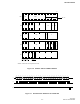
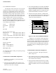
The main subassemblies of this transceiver are
the RF board, VCO board, TCXO, Loader board or
Modem. A block diagram of the transceiver is located
in Figure 4-1. The 3492 is also available in Transmit
only and Receive only models.
The 3492 has a reference oscillator stability of
±1.5 PPM. The 17.5 MHz TCXO (Temperature Com-
pensated Crystal Oscillator) is soldered directly to the
RF board. The TCXO is not serviceable.
4.1.2 SYNTHESIZER
The VCO (voltage-controlled oscillator) output
signal is the receiver first injection frequency in the
Receive mode and the transmit frequency in the
Transmit mode. The first injection frequency is
87.85 MHz below the receive frequency. The fre-
quency of this oscillator is controlled by a DC voltage
produced by the phase detector in synthesizer chip
U800.
Channels are selected by programming counters
in U800 to divide by a certain number. This program-
ming is performed over a serial bus formed by the
Synth Clock, Synth Enable, and Data pins of J201.
This programming is performed by the Loader board,
modem or user supplied hardware and software (see
Section 3).
The frequency stability of the synthesizer in both
the receive and transmit modes is established by the
stability of the TCXO. The TCXO is stable over a
temperature range of -30° to +60° C (-22° to +140° F).
4.1.3 RECEIVER
The receiver is a double-conversion type with
intermediate frequencies of 87.85 MHz / 450 kHz.
Bandpass filters reject the image, half IF, injection,
and other unwanted frequencies. A four-pole crystal
filter enhances receiver selectivity.
4.1.4 TRANSMITTER
The transmitter produces a nominal RF power
output of 5W at 13.3V DC, adjustable down to 1W.
Frequency modulation of the transmit signal occurs in
the synthesizer. Transmit audio processing circuitry is
contained in the Loader board, modem or customer-
supplied equipment.
4.2 SYNTHESIZER
Programming of the synthesizer provides the data
necessary for the internal prescaler and counters. One
input signal is the reference frequency. This frequency
is produced by the 17.5 MHz reference oscillator
(TCXO). The other input signal is the VCO
frequency.
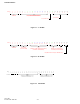
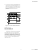
A block diagram of the synthesizer is shown in
Figure 4-1 and a block diagram of Synthesizer IC
U800 is shown in Figure 4-2. As stated previously,
the synthesizer output signal is produced by a VCO
(voltage controlled oscillator). The VCO frequency is
controlled by a DC voltage produced by the phase
detector in U800. The phase detector senses the phase
and frequency of the two input signals and causes the
VCO control voltage to increase or decrease if they
are not the same. The VCO is then "locked" on
frequency.