
User Manual


PROGRAMMING
3-6
June 1997
Part No. 001-3492-001
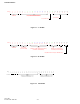
3.2.8 RADIO DIAGNOSTICS
The diagnostic features allow the user to program
a Digital-To-Analog Converter (DAC) to adjust RF
output power and modulation flatness without remov-
ing the radio from the enclosure. Bit "a0" can be set
to provide an analog voltage representative of the for-
ward and reverse RF power at the radio interface con-
nector J201, pin 14. This feature can be used to moni-
tor the condition of the transceiver and antenna/
feedline. Figure 3-7 is a diagram of the Diagnostic
Serial Data Stream with definitions of the bits. It is 19
bits long, the front (MSBs) can be padded with "Don’t
Cares" (XXs) to get to 24 bits.
Clock 1 MHz (max)
Diag Enable 250 ns (min)
XX Don’t Care
DAC Bits
A1-A0 = DAC Output Select
00=Power Set Data=0x00 to 0xFF, RNG=1
01=Mod Adj Data=0x00 to 0xFF, RNG=1
11=DAC Control Select Data=0x00 to 0xFF, RNG=1
RNG = Range Select (max output) (Ref=5.5V÷2)
0 = 1 x Ref
1 = 2 x Ref
D7-D0 = D/A Data
0x00 = 0.0V
0xFF = 1 x Ref (RNG=0)
0xFF = 2 x Ref (RNG=1)
Shift Register Bits:
a0 = Diagnostic Select to J201, pin 14 (Analog Voltage)
0 = Forward Power
1 = Reverse Power
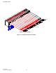
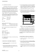
3.3 RECEIVE TO TRANSMIT SEQUENCE
1. Synthesizer is loaded (D, C, B and A0 words).
Refer to Figure 3-8.
2. The state of the RX_EN line does not have to be
changed until the last bit is sent. However, Recieve
will cease as soon as it is changed.
3. The SYNTH ENABLE line should be held HIGH
for 2 to 3 milliseconds after the last word is sent.
This puts the frequency synthesizer in a SPEEDUP
MODE and slightly improves lock times then the
Synth Enable should be returned to a low state.
4. After the last word is strobed in, 7 milliseconds
(worst case) should elapse before TX_EN is turned
ON. This allows the synthesizer to come within
1 kHz of the desired frequency.
Figure 3-8 RX TO TX TIMING DIAGRAM
"Ramp-Up" is the amount of time required for
the transmitter to reach full power once the TX EN
has been applied. The Ramp-Up circuitry (located on
the transceiver) minimizes adjacent channel interfer-
ence caused by spectral spreading (sinx/x) when the
transmitter is keyed. The Ramp-Up time is approxi-
mately 3 ms.
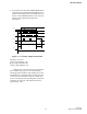
3.4 TRANSMIT TO RECEIVE SEQUENCE
1. TX_EN is turned OFF. This signal is shaped.
Refer to Figure 3-9.
2. The synthesizer load process could begin slightly
before, but when the last bit is strobed in the synthe-
sizer it will become unlocked.
3. The RX_EN line should switch from low to high
AFTER the TX_EN is switched. The RX_EN not
only turns the RX circuits on but also Pin Shifts the
VCO.
D0D24D0 D24 D0 D24
"D" WORD "B" WORD "A" WORD
DATA
CLOCK
t=0
SPEEDUP
RAMP-UP
LOCK
RX_EN
SYNTH_EN
9V TX
TX_EN
"C" WORD