
User Manual


3-1
June 1997
Part No. 001-3492-001
SECTION 3 PROGRAMMING
3.1 INTRODUCTION
DM3492 - The information in Section 3.2
describes synthesizer programming protocol. This
information can be used as a basis for designing the
synthesizer programming hardware and software
required.
3.2 DM3492 SYNTHESIZER DATA PROTOCOL
3.2.1 GENERAL
The 928-960 MHz band is divided into two seg-
ments for the purpose of reducing VCO gain. The
"LOW" band covers the 928-944 MHz segment and
the "HIGH" band covers the 944-960 MHz segment.
The VCO band selection is accomplished by capaci-
tive pin-switching. The band switching is imple-
mented in both the transmit and receive modes. The
front-end filters and transmitter line-up cover the
entire 928-960 MHz band without adjustment.
Receive Bandwidth 928-960 MHz
Transmit Bandwidth 928-960 MHz
First IF 87.850 MHz
Second IF 450.0 kHz
First LO Injection 840.150-872.150 MHz*
Second LO Injection 87.40 MHz*
TCXO Frequency 17.50 MHz
Resolution 6.25 kHz
Loop Comparison Freq. 50 kHz
* Low Side Injection
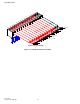
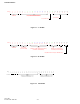
A diagram of the 32 Bit Synthesizer Serial Data
Stream with definitions of the bits is shown in Figure
3-1.
Clock 1 MHz (max)
Synth Enable 250 ns (min) (for D, C and B words
approximately 3 ms for A0 word)
D00-D23 D, C, B and A0 words
3.2.2 SYNTHESIZER DATA
In order to implement the band selection and
Tx/Rx frequency shift mentioned in Section 3.2.1, an
additional shift register was added to the synthesizer
section. Therefore, an additional 8 Bits of data are
added to each of the synthesizer load words (D/C/B/
A0) as shown in the serial data stream in Figure 3-1.
3.2.3 D-WORD CALCULATION (24 BITS)
The D-Word programs the Main, Reference and
Auxiliary dividers, and sets the modulus (refer to
Figures 3-2 and 3-6).
NR = 350 Ftcxo/50 kHz=350
where Ftcxo=17.5 MHz
SM = 00 Reference select for main phase detector
EM = 1 Main divider enable flag
SA = 00 Reference select for aux phase detector
EA = 1 Auxiliary divider enable flag
FMOD = 1 Selects modulus 8
LONG = 0 Send all 4 words with A0
D Word = 0xA1 0x5E 0x26
Figure 3-1 32-BIT SYNTHESIZER SERIAL DATA STREAM
D1 D0
XXXX
XX
XX
LSB (00)
Data
Clock
Synth En
MSB (31)
D23 D22 D21 D20 - - Tx-Tx+Low-
Low+