
User Manual


2-1
June 1997
Part No. 001-3492-001
SECTION 2 INSTALLATION
2.1 PRE-INSTALLATION CHECKS
Field alignment should not be required before the
3492 is installed. However, it is still good practice to
check the performance to ensure that no damage
occurred during shipment. Performance tests are
located in Section 6.2.
2.2 INTERFACING WITH DATA EQUIPMENT
2.2.1 DM3492 (RF Board)
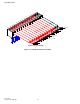
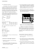
Connector J201 on the data transceiver PC board
provides the interface with the data equipment. This is
a 14-pin female connector with .025" square pins on
0.1" centers (Dupont 76308-114). The cable (Part No.
023-3472-007) is not included with the data trans-
ceiver. An interface cable diagram and pin designa-
tions are shown in Figure 2-1.
The following is a general description of the
input and output signals on Transceiver Interface con-
nector J201.
Pin 1 (Ground) - Chassis ground.
Pin 2 (+13.3V DC) - Input, transceiver main power.
Input range 10-16V DC with ±3 dB variation in output
power.
Pin 3 (Tx En) - Input +3-16V DC. Enables transmit
circuitry. ≤ 0.3V DC in Rx mode.
Pin 4 (Rx En) - Input +3-16V DC. Enables receive cir-
cuitry. ≤ 0.3 V DC in Tx mode.
Pin 5 (RF En) - Input +3-16V DC. Shuts down on-
board regulators. To be used as a power save mode.
Pin 6 (Mod In) - Provides a response of ±2 dB from
DC to 5 kHz across the RF band (referenced to
1 kHz). It is programmable to 1 dB with the diagnostic
DAC. The modulation capability is 250 mV RMS
±3 dB that produces ±5 kHz deviation with a 1 kHz
tone. When this input is used, a temperature compen-
sated 2.5V DC bias is required as variations in voltage
cause the frequency to change. The transceiver regula-
tory compliance must be applied for with the customer
supplied modulation limiting/filter circuit and chassis.
Pin 7 (Synth Lock) - Output from synthesizer lock de-
tect circuit. Low (< 1V DC) = unlocked, high (>2.5V
DC) = locked.
Pin 8 (Synth En) - TTL input. Latch enable signal for
synthesizer. 250 ns min. for D, C and B words; 3 ms
min. for A0 word. A rising edge latches the data loaded
into the synthesizer IC..
Pin 9 (Data) - TTL input. Serial data line used for pro-
gramming the synthesizer and diagnostic functions.
Pin 10 (Synth Clock) - TTL input. Clock signal for se-
rial data input on Pin 9. Data is valid on the rising edge.
1 MHz max. frequency.
Pin 11 (Diag En) - TTL input. Loads programmed
DAC values into DAC (U900) for modulation adjust
and power set. Also provides the strobe signal for shift
register (u901) for selecting Forward and Reverse pow-
er diagnostics. 250 ns min. activates on rising edge.
Pin 12 (RSSI) - Analog output (0.5-2V DC). The Re-
ceive Signal Strength Indicator output provides a volt-
age that increases in proportion to the strength of the
RF input signal.
Pin 13 (Demod) - Analog output. The Receiver De-
mod output level is 150 mV RMS with a modulation
signal of 1 kHz at 60% of maximum deviation. The out-
put is DC coupled and referenced to +2.5V DC. Load
impedance should be >10k ohms.
Pin 14 (Diag) - Analog Output. This pin is enabled by
pin 11. When the Loader board is used it has the capa-
bility to test the operating environment through diag-
nostics. The diagnostic capabilities are in Section 1.2.2