
User Manual


CIRCUIT DESCRIPTION
4-7
Part No. 001-3422-003
4.2.7 SYNTHESIZER INTEGRATED CIRCUIT (U811)
Introduction
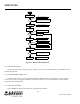
Synthesizer chip U811 is shown in Figure 4-2. This device contains the following circuits: R (reference),
Fractional-N, NM1, NM2 and NM3; phase and lock detectors, prescaler and counter programming circuitry. The
basic operation was described in Section 4.2.1.
Channel Programming
Frequencies are selected by programming the R, Fractional-N, NM1, NM2 and NM3 in U811 to divide by a
certain number. These counters are programmed by Loader board or a user supplied programming circuit. More
information on programming is located in Section 3.
As previously stated, the counter divide numbers are chosen so that when the VCO is oscillating on the
correct frequency, the VCO-derived input to the phase detector is the same frequency as the reference oscillator-
derived frequency.
The VCO frequency is divided by the internal prescaler and the main divider to produce the input to the phase
detector.
4.2.8 LOCK DETECT
When the synthesizer is locked on frequency, the SYNTH LOCK output of U811, pin 18 (J201, pin 7) is a
high voltage. When the synthesizer is unlocked, the output is a low voltage. Lock is defined as a phase difference
of less than 1 cycle of the TCXO.
4.3 RECEIVER CIRCUIT DESCRIPTION
4.3.1 PRESELECTOR FILTER, RF AMPLIFIER (Q202)
Capacitor C201 couples the receive signal from the antenna switch to the LC preselector filter composed of
L201-L203, CR281, CR282, C202-C207. (The antenna switch is described in Section 4.4.4.) The preselector
filter is a 2-pole discrete LC varactor tuned bandpass filter adjusted to pass only a narrow band of frequencies to
the receiver. This attenuates the image and other unwanted spurious frequencies.
The preselector filter is tuned in frequency by varying the reverse bias voltage of varactors CR281/CR282.
The filter control voltage is either generated by Digital to Analog Converter (DAC) U911 or R920 and amplified
by U831 to generate a higher voltage swing to the varactors and minimize filter loss. R206 and capacitors C281-
C285 filter the varactor voltage and provide RF isolation. The control voltage source is chosen by U913.
Impedance matching between the helical filter and RF amplifier Q202 is provided by C207 and L204. CR201
protects the base-emitter junction of Q202 from excessive negative voltages that may occur during high signal
conditions. Q201 is a switched constant current source which provides a base bias for Q202. Q201 base bias is
provided by R202/R203. Current flows through R201 so that the voltage across it equals the voltage across R202
(minus the base-emitter drop of Q201). In the transmit mode the receive +9.6V is removed and Q201 is off.