
User Manual

CIRCUIT DESCRIPTION
4-6
Part No. 001-3422-003
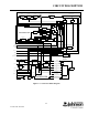
4.2.3 CASCODE AMPLIFIERS/VCO (Q871/Q872)
The output signal on the collector of Q871 is coupled to buffer amplifier Q872 which forms a cascade
amplifier. This is a shared-bias amplifier which provides amplification and also isolation from the stages that
follow. The signal is coupled and matched from the collector of Q872 through inductors and capacitors and a
T-pad to amplifier Q882.
4.2.4 AMPLIFIER (Q882)
Amplifier Q882 provides final amplification of the VCO signal. Bias for Q882 is provided by Q881 and
several resistors. Matching to the transmitter and receive first injection is provided by L891 and C892. A 6 dB
T-pad is used to isolate the transmitter and receive first injection.
4.2.5 VOLTAGE FILTER (Q901)
Q901 on the RF board is a capacitance multiplier to provide filtering of the 8.6V supply to the VCO. R901
provides transistor bias and C901 provides the capacitance that is multiplied. If a noise pulse or other voltage
change appears on the collector, the base voltage does not change significantly because of C901. Therefore, base
current does not change and transistor current remains constant. CR901 decreases the charge time of C901 when
power is turned on. This shortens the start-up time of the VCO. C902 and C903 are RF decoupling capacitors.
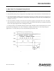
4.2.6 VCO FREQUENCY SHIFT (Q841)
The VCO must be capable of producing frequencies from approximately 132-195.45 MHz to produce the
required receive injection and transmit frequencies. If this large of a shift was achieved by varying the VCO
control voltage, the VCO gain would be undesirably high. Therefore, capacitance is switched in and out of the
tank circuit to provide a coarse shift in frequency.
This switching is controlled by the T/R pin shift (RX_EN) on J201, pin 4, Q841/Q842 and pin diode CR851.
When a pin diode is forward biased, it presents a very low impedance to RF; and when it is reverse biased, it
presents a very high impedance. The capacitive leg is switched in when in transmit and out when in receive.
When J201, pin 4 is high in receive (+5V), Q173 is turned on and the collector voltage goes low. A low on
the base of Q172 turns the transistor on and the regulated +9.6V on the emitter is on the collector for the receive
circuitry. Q171 applies a low on the base of Q841, the transistor is off and the collector is high. With a high on the
base of Q842 and a low on the emitter, this reverse biases CR851 for a high impedance.
The capacitive leg on the VCO board is formed by C852, CR851 and C853. When J201, pin 4 is low in
transmit, Q842 is turned on and a high is on the emitter, Q171 is turned off and the collector voltage goes high. A
low on the base of Q173 turns the transistor off and the regulated +9.6V is removed from the receive circuitry.
With a high on the base of Q841 the transistor is on and the collector is low. With a low on the collector of Q842
and a high on the emitter, this forward biases CR851 and provides an RF ground through C852 and C853 is
effectively connected to the tank circuit. This decreases the resonant frequency of the tank circuit.