
User Manual


SECTION 4
4-1
Part No. 001-3422-003
CIRCUIT DESCRIPTION
4.1 GENERAL
4.1.1 INTRODUCTION
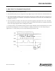
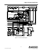
The main subassemblies of this transceiver are the RF board, VCO board, TCXO and Loader board. A
block diagram of the transceiver is located in Figure 4-1.
The 3422 is available with a reference oscillator stability of ±2.5 PPM. The TCXO (Temperature
Compensated Crystal Oscillator) is soldered directly to the RF board. The TCXO is not
serviceable.
4.1.2 SYNTHESIZER
The VCO (voltage-controlled oscillator) output signal is the receiver first injection frequency in the Receive
mode and the transmit frequency in the Transmit mode. The first injection frequency is 21.45 MHz above the
receive frequency. The frequency of this oscillator is controlled by a DC voltage produced by the phase detector
in synthesizer chip U811.
Channels are selected by programming counters in U811 to divide by a certain number. This programming
is performed over a serial bus formed by the Synth Clock, Synth Enable, and Synth Data pins of J201. This
programming is performed by the Loader board or user supplied hardware and software (see Section 3).
The frequency stability of the synthesizer in both the receive and transmit modes is established by the
stability of the reference oscillator described in the preceding section. These oscillators are stable over a
temperature range of -30° to +60° C (-22° to +140° F).
Table 4-1 Reference Frequency
Band Frequency
Band 6 17.5 MHz
Band 5 14.85 MHz
Band 4 14.85 MHz