
User Manual

INSTALLATION
-2
Part No. 001-3422-003
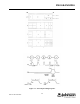
Pin 8 (Synth En) - TTL input. Latch enable signal for synthesizer. 250 ns min. for D, C and B words; 3 ms min.
for A0 word. A rising edge latches the data loaded into the synthesizer IC..
Pin 9 (Data) - TTL input. Serial data line used for programming the synthesizer and diagnostic functions.
Pin 10 (Synth Clock) - TTL input. Clock signal for serial data input on Pin 9. Data is valid on the rising edge. 1
MHz max. frequency.
Pin 11 (Diag En) - TTL input. Loads programmed DAC values into DAC (U911) for modulation adjust and power
set. Also provides the strobe signal for shift register (u901) for selecting Forward and Reverse power diagnostics.
250 ns min. activates on rising edge.
Pin 12 (RSSI) - Analog output (0.5-2V DC). The Receive Signal Strength Indicator output provides a voltage that
increases in proportion to the strength of the RF input signal.
Pin 13 (Demod) - Analog output. The Receiver Demod output level is 150 mV RMS with a modulation signal of 1
kHz at 60% of maximum deviation. The output is DC coupled and referenced to +2.5V DC. Load impedance should
be >10k ohms.
Pin 14 (Diag) - Analog Output. This pin is enabled by pin 11. When the Loader board is used it has the capability
to test the operating environment through diagnostics. The diagnostic capabilities are in Section 1.2.2