
User Manual

SECTION 2
2-1
Part No. 001-3422-003
INSTALLATION
1.1 PRE-INSTALLATION CHECKS
Field alignment should not be required before the 3422 is installed. However, it is still good practice to
check the performance to ensure that no damage occurred during shipment. Performance tests are located in
Section 6.2.
1.1 INTERFACING WITH DATA EQUIPMENT
1.1.1 DM-3422 (RF Board)
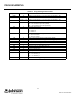
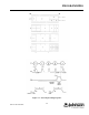
Connector J201 on the data transceiver PC board provides the interface with the data equipment. This is a
14-pin female connector with .025" square pins on 0.1" centers (Dupont 76308-114). The cable (Part No. 023-
3472-007) is not included with the data transceiver. An interface cable diagram and pin designations are shown
in Figure 2-1.
The following is a general description of the input and output signals on Transceiver Interface connector
J201.
Pin 1 (Ground) - Chassis ground.
Pin 2 (+13.3V DC) - Input, transceiver main power. Input range 10-16V DC with ±3 dB variation in output power.
Pin 3 (Tx En) - Input +3-16V DC. Enables transmit circuitry. ≤ 0.3V DC in Rx mode.
Pin 4 (Rx En) - Input +3-16V DC. Enables receive circuitry. ≤ 0.3 V DC in Tx mode.
Pin 5 (RF En) - Input +3-16V DC. Shuts down on-board regulators. To be used as a power save mode.
Pin 6 (Mod In) - Provides a response of ±2 dB from DC to 5 kHz across the RF band (referenced to
1 kHz). It is programmable to 1 dB with the diagnostic DAC. The modulation capability is 250 mV RMS
±3 dB that produces ±5 kHz deviation with a 1 kHz tone. When this input is used, a temperature compensated
2.5V DC bias is required as variations in voltage cause the frequency to change. The transceiver regulatory
compliance must be applied for with the customer supplied modulation limiting/filter circuit and chassis.
Pin 7 (Synth Lock) - Output from synthesizer lock detect circuit. Low (< 1V DC) = unlocked, high (>2.5V DC)
= locked.