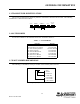
SYNTHESIZED VHF TELEMETRY UNIT PART NO. 242-3422-XYZ Third Printing September 1998 Supersedes 001-3422-002 February 1998 Part No. 001-3422-003 U.S.A.
SYNTHESIZED VHF TELEMETRY UNIT PART NO. 242-3422-XYZ Copyright 1998 by the Johnson Data Telemetry Corporation. The Johnson Data Telemetry Corporation designs and manufactures radios and radio modems to serve a wide variety of data communication needs. The Johnson Data Telemetry Corporation produces equipment for the fixed data market including SCADA systems for utilities, petrochemical, waste and fresh water management markets and RF boards for OEM applications in the Radio Frequency Data Capture market.
TABLE OF CONTENTS 1 GENERAL INFORMATION 1.1 1.2 1.3 1.4 1.5 1.6 1.7 1.8 1.9 SCOPE OF MANUAL . . . . . . . . . . . . . . . . . . . . . . . . . . . . . . . . . . . . . . . . . . . . . . . . . . . . . . . . . . . . . . . . . . . . . . . 1-1 EQUIPMENT DESCRIPTION. . . . . . . . . . . . . . . . . . . . . . . . . . . . . . . . . . . . . . . . . . . . . . . . . . . . . . . . . . . . . . . . 1-1 GENERAL . . . . . . . . . . . . . . . . . . . . . . . . . . . . . . . . . . . . . . . . . . . . . . . . . . . . . . .
SECTION 1 GENERAL INFORMATION 1.1 SCOPE OF MANUAL This service manual contains alignment and service information for the Johnson Data Telemetry (JDT) DM3422 VHF Synthesized Telemetry Unit. This manual concentrates on the RF section of the Data Link (DL) which may be paired with an internal Loader board or 9600 baud Modem board. Service manuals addressing items specific to the Loader board (Part No. 001-3240-003) and the Modem board (Part No.
GENERAL INFORMATION 1.2.2 DL-3422 WITH LOADER BOARD The DL-3422 includes the 8-channel Loader board (Part No. 023-3240-001), which performs synthesizer loading through an RS-232 DB-9 interface.
GENERAL INFORMATION 1.3 TRANSCEIVER IDENTIFICATION The transceiver identification number is printed on a label that is affixed to the PC board. The following information is contained in that number: Model 3422 Ninth Digit of PN Revision Letter 2 Manufacture Date Plant Warranty Number 14 3 A 12345 A Week No. of Year Year 1.4 ACCESSORIES Accessories available for the 3422 data transceiver are listed in Table 1-1. Table 1-1 ACCESSORIES Accessory Part No.
GENERAL INFORMATION 1.6 FACTORY CUSTOMER SERVICE The Customer Service Department at JDT provides customer assistance on technical problems and the availability of local and factory repair facilities. Customer Service hours are 7:30 a.m. - 4:30 p.m. Central Time, Monday - Friday.
GENERAL INFORMATION You can send your order by mail or FAX (see Section 1.6 for mailing address). Mail orders should be sent to the Service Parts Department. FAX Machine - Sales (507) 835-6648 1.9 IF A PROBLEM ARISES... JDT products are designed for long life and failure-free operation. If a problem arises, factory service is available. Contact the Customer Service Department before returning equipment. A service representative may suggest a solution eliminating the need to return equipment. 1.9.
GENERAL INFORMATION 3422 UHF SYNTHESIZED TELEMETRY UNIT SPECIFICATIONS The following are general specifications intended for use in testing and servicing this transceiver. For current advertised specifications, refer to the specification sheet available from the Marketing Department. Specifications are subject to change without notice.
GENERAL INFORMATION Discriminator Output Output Bias Output Impedance Data Characteristics RSSI TRANSMITTER Frequency Stability Bandwidth Maximum System Deviation Modulation Input Bias Input Impedance Distortion Capability Flatness DAC) RF Power Output Deviation Symmetry RF Output Impedance Duty Cycle Transmitter Adjacent Power Intermodulation Attenuation Spurious and Harmonic FM FM Hum and Noise +1/-3 dB from DC to 5 kHz (reference to 1 kHz)(30 kHz BW) +1/-3 dB from DC to 3.0 kHz 15 MHz BW 2.5V DC ±0.
GENERAL INFORMATION This page left intentionally blank. 1-8 Part No.
SECTION 2 INSTALLATION 1.1 PRE-INSTALLATION CHECKS Field alignment should not be required before the 3422 is installed. However, it is still good practice to check the performance to ensure that no damage occurred during shipment. Performance tests are located in Section 6.2. 1.1 INTERFACING WITH DATA EQUIPMENT 1.1.1 DM-3422 (RF Board) Connector J201 on the data transceiver PC board provides the interface with the data equipment. This is a 14-pin female connector with .025" square pins on 0.
INSTALLATION Pin 8 (Synth En) - TTL input. Latch enable signal for synthesizer. 250 ns min. for D, C and B words; 3 ms min. for A0 word. A rising edge latches the data loaded into the synthesizer IC.. Pin 9 (Data) - TTL input. Serial data line used for programming the synthesizer and diagnostic functions. Pin 10 (Synth Clock) - TTL input. Clock signal for serial data input on Pin 9. Data is valid on the rising edge. 1 MHz max. frequency. Pin 11 (Diag En) - TTL input.
SECTION 3 PROGRAMMING 3.1 INTRODUCTION The DL-3422 information in Section 3.2 describes synthesizer programming protocol. This information can be used as a basis for designing the synthesizer programming hardware and software. The DL-3422 VHF Transceiver uses a high performance Fractional-N Synthesizer and Voltage Controlled Oscillator (VCO). The Fractional-N Synthesizer offers high frequency resolution, fast lock times, and improved noise performance over conventional synthesis techniques.
PROGRAMMING Table 3-1 Programming Function Table Symbol Bits NM1 NM2 NM3 PR 12 8 if PR = “01” 4 if PR = “10” 4 if PR = “10” 2 NF FMOD 3 1 LONG 1 CN CL CK EM EA SM SA NR NA PA 8 2 4 1 1 2 2 12 12 1 Function Number of main divider cycles when prescaler modulus = 64* Number of main divider cycles when prescaler modulus = 65* Number of main divider cycles when prescaler modulus = 72* Prescaler type in use PR = “01”: modulus 2 prescaler (64/65) PR = “10”: modulus 3 prescaler (64/65/72) Fractional-N inc
PROGRAMMING Figure 3-2 Serial Input Word Format Figure 3-3 Serial Input Timing Sequence 3-3 Part No.
PROGRAMMING Table 3-2 Serial Interface Specifications Symbol Parameter Test Conditions fCLOCK Clock Frequency tSU Set-up time: DATA to CLOCK CLOCK to STROBE tH Hold Time: CLOCK to DATA tW Pulse width; CLOCK Pulse width; STROBE tSW Limits MIN TYP MAX 10 B, C, D words A word, PR = "01" Pulse width; STROBE A word, PR = "10" Units MHz 30 30 30 30 1 . (NM2 . 65) + tW f VCO ns ns ns ns 1 . [(NM2 . 65) + (NM3 + 1 . 72] + tW fVCO 3.2.
PROGRAMMING C-WORD The C-Word programs the Auxiliary (2nd LO injection frequency) and selects auxiliary preselector mode. PA = 1 NA = 584 (for 7.5 kHz resolution) NA = 438 (for 6.25 kHz resolution NA = 876 (for 5.0 kHz resolution) NA = 1095 (for 2.5 kHz resolution) NOTE: applies to Band 6 only. Where: NA = LO2 ÷ FCM B-WORD The B-Word programs the Fractional-N charge pump current factor (CN), the binary acceleration factors (CL/ CK) and the prescaler modulus.
PROGRAMMING THE A0-WORD The A0 Word is sent last. the A0 word contains the programming information for the main dividers. The A0 word consists of four divider parameters, NM1, NM2, NM3, and NF described below. After clocking the A0 word, the STROBE line is held high for approximately 3 ms to place the synthesizer in “speed-up” mode to decrease lock times.
PROGRAMMING C-Word calculation: NA = 1095 (Decimal) PA = 1 C-Word (Hex) = 94 47 80 B-Word calculation: CN = 95 (Decimal from Table 3-3) CK = 0000 CL = 00 PR = 10 B-Word (Hex) = 80 5F 2 A0-Word calculation: When the D-Word is programmed with FMOD = 8 and NR = 875 as described above, the fractional increment resolution is FCM ÷ FMOD = 20 kHz ÷ 8 = 2.5 kHz. Where FCM = FREF ÷ NR = 17.5 MHz ÷ 875 = 20 kHz.
PROGRAMMING NM1 = INT {N ÷ 64} - NM2 - NM3 - 3 = 134 - 7 - 4 - 3 = 120 NF = FRAC {LO ÷ FCM} x FMOD = FRAC {171.4625 ÷ 0.02} x 8 = 0.125 x 8 =3 Where INT = Integer Part FRAC = Fractional Part 3-8 Part No.
PROGRAMMING 3.3 RECEIVE TO TRANSMIT SEQUENCE 1. Load the synthesizer (D, C, B and A0 words). 2. The RX Enable (J201, pin 4) is changed from a logic high to logic low after the last bit of the A0 Word is sent. 3. The SYNTH ENABLE (SYNTH_EN) should be held in a high state for 3 milliseconds after the A0 Word is sent. This puts the synthesizer in a temporary “speedup mode” which improves lock times. Then, the SYNTH_EN is returned to a low state. 4.
PROGRAMMING 3.4 TRANSMIT TO RECEIVE SEQUENCE 1. Unkey the transmitter by bringing the 7.5 TX low. 2. Allow 3 ms for “ramp-down” 1 after the 7.5 TX is brought low. 3. Apply a logic high to the RX Enable line. 4. Load the synthesizer receive frequency. The SYNTH Enable line should be held high for 3 ms on the last word to place the synthesizer in speedup mode for faster lock times. The SYNTH Enable line should then be returned to logic low. 5.
Figure 3-5 TX TO RX TIMING DIAGRAM June 1997 -
SECTION 4 CIRCUIT DESCRIPTION 4.1 GENERAL 4.1.1 INTRODUCTION The main subassemblies of this transceiver are the RF board, VCO board, TCXO and Loader board. A block diagram of the transceiver is located in Figure 4-1. The 3422 is available with a reference oscillator stability of ±2.5 PPM. The TCXO (Temperature Compensated Crystal Oscillator) is soldered directly to the RF board. The TCXO is not serviceable. Table 4-1 Reference Frequency Band Frequency Band 6 Band 5 Band 4 17.5 MHz 14.85 MHz 14.
CIRCUIT DESCRIPTION 4.1.3 RECEIVER The receiver is a double-conversion type with intermediate frequencies of 21.45 MHz / 450 kHz. Varactor tuned LC bandpass filters reject the image, half IF, injection, and other unwanted frequencies. A four-pole crystal filter enhances receiver selectivity. 4.1.4 TRANSMITTER The transmitter produces a nominal RF power output of 5W at 13.3V DC, adjustable down to 1W. Frequency modulation of the transmit signal occurs in the synthesizer.
CIRCUIT DESCRIPTION RF BPF RF AMP RF BPF CR281/CR282 Q201/Q202 CR281/CR282 MIXER Q231/Q232 21.
CIRCUIT DESCRIPTION CLOCK DATA STROBE Vss SERIAL INPUT + PROGRAM LATCHES EM RF IN RF IN PR NM1 NM2 NM3 2 12 8 FB FB 2 64/65/72 PRESCALER V DD FMOD NF 3 FRACTIONAL ACCUMULATOR MAIN DIVIDERS PRESCALER MODULUS CONTROL RF RN CN 8 TEST EM SM 2 NR EM+EA NORMAL OUTPUT CHARGE PUMP MAIN PHASE DETECTOR CL 2 PHP SPEED-UP OUTPUT CHARGE PUMP MAIN REFERENCE SELECT CK 12 4 REF IN REFERENCE DIVIDER SA 2 PA EA AUX IN NA EA +2 +2 INTEGRAL OUTPUT CHARGE PUMP +2 RA SECONDARY REFERENCE SE
CIRCUIT DESCRIPTION Frequency Control and Modulation The VCO frequency is controlled in part by DC voltage across varactor diodes CR852, CR853 and CR854. As voltage across a reverse-biased varactor diode increases, its capacitance decreases. Therefore, VCO frequency increases as the control voltage increases. CR852/CR853 and CR854 are paralleled varactors to divide the capacitance and improve linearity. The varactors CR852/CR853 are biased at -2.0V so the control line voltage can operate closer to ground.
CIRCUIT DESCRIPTION 4.2.3 CASCODE AMPLIFIERS/VCO (Q871/Q872) The output signal on the collector of Q871 is coupled to buffer amplifier Q872 which forms a cascade amplifier. This is a shared-bias amplifier which provides amplification and also isolation from the stages that follow. The signal is coupled and matched from the collector of Q872 through inductors and capacitors and a T-pad to amplifier Q882. 4.2.4 AMPLIFIER (Q882) Amplifier Q882 provides final amplification of the VCO signal.
CIRCUIT DESCRIPTION 4.2.7 SYNTHESIZER INTEGRATED CIRCUIT (U811) Introduction Synthesizer chip U811 is shown in Figure 4-2. This device contains the following circuits: R (reference), Fractional-N, NM1, NM2 and NM3; phase and lock detectors, prescaler and counter programming circuitry. The basic operation was described in Section 4.2.1. Channel Programming Frequencies are selected by programming the R, Fractional-N, NM1, NM2 and NM3 in U811 to divide by a certain number.
CIRCUIT DESCRIPTION This removes the bias from Q202 and disables the RF amplifier in transmit mode. This prevents noise and RF from being amplified by Q202 and fed back on the first injection line. Additional filtering of the receive signal is provided by a three pole discrete LC varactor tuned bandpass filter composed of filter L212-L214, L221-L224, CR283-CR285, C214-C217, C221-C223. L211 and C213 provide impedance matching between Q202 and this filter.
CIRCUIT DESCRIPTION C234 52.95 MHz MIXER 1 20 2 19 C267 18 NC 52.5 MHz 3 4 17 OSCILLATOR IF AMP 5 RSSI OUTPUT + 16 RSSI MIXER OUT IF DEC2 IF AMP IN IF DEC1 IF AMP OUT 15 V CC AUDIO FB 6 14 7 8 AUDIO OUTPUT VREG - LIMITER + RSSI FB 9 10 13 LIMITER IN LIMITER DEC1 12 QUAD LIMITER DEC2 11 LIMITER OUT L253 Figure 4-3 U241 Block Diagram 4.3.
CIRCUIT DESCRIPTION Limiter-Amplifier The output of Z241/Z242 is applied to a limiter-amplifier circuit in U241. This circuit amplifies the 450 kHz signal and any noise present; then limits this signal to a specific value. When the 450 kHz signal level is high, noise pulses tend to get clipped off by the limiter; however, when the 450 kHz signal level is low, the noise passes through the limiter. C275/C276 decouple the 450 kHz signal.
CIRCUIT DESCRIPTION 4.4.3 FINAL (U531), COMPARATOR (U111C) RF module U531 has an RF output of 1W to 5W and operates on an input voltage from 10-16V. Power control is provided by U581, U111, Q531 and a directional coupler A531. The power is adjusted by Power Set Control R535 that provides a reference voltage to U111C. U111C drives Q531 and PA module U531. One end of the Balun directional coupler is connected to a forward RF peak detector formed by R591, CR591, C591 and U581A.
CIRCUIT DESCRIPTION 4.4.5 TRANSMITTER KEY-UP CONTROL Q121, Q122 and Q123 act as switches which turn on with the RX_EN line. When the line goes low Q121 is turned off, which turns Q122 on, turning Q123 on. This applies 13.6V to U111 before the TX_EN line goes high. U111A/B provide the key-up and key-down conditioning circuit. C116 and R117 provide a ramp-up and ramp-down of the 9V transmit supply during key-up and key-down which reduces load pull of the VCO during key-up.
SECTION 5 SERVICING 5.1 GENERAL 5.1.1 PERIODIC CHECKS This transceiver should be put on a regular maintenance schedule and an accurate performance record maintained. Important checks are receiver sensitivity and transmitter frequency, modulation, and power output. A procedure for these and other tests is located in Section . It is recommended that transceiver performance be checked annually even though periodic checks are not required by the FCC.
SERVICING When the VCO is unlocked, the fR and fV inputs to the phase detector are usually not in phase (see Section 4.1.2). The phase detector in U811 then causes the VCO control voltage to go to the high or low end of its operating range. This in turn causes the VCO to oscillate at the high or low end of its frequency range. As shown in Figure 4-1, a loop is formed by VCO Q872, amplifier Q871, and the RF IN of U811.
SERVICING 5.3 RECEIVER SERVICING To isolate a receiver problem to a specific section, refer to the troubleshooting flowchart in Figure 5-1. Tests referenced in the flowchart are described in the following information. NOTE: Supply voltages are provided by the user. 5.3.1 SUPPLY VOLTAGES AND CURRENT Measure the supply voltages on the following pins at interface connector J201: Pin 4 - 5.0V DC Receive Pin 5 - 5.
SERVICING START MEASURE CURRENT AND VOLTAGES REFER TO SECTION 5.3 NO OK ? CHECK FUSES AND WIRE HARNESS CONNECTIONS YES CHECK MIXER/ DETECT CIRCUIT REFER TO SECTION 5.3.2 CHECK DATA OUTPUT REFER TO SECTION 5.3.2 OK ? NO CHECK U241 YES CHECK AUDIO CIRCUIT REFER TO SECTION 5.3.4 REFER TO SECTION 5.3.3 OK ? NO REPLACE DEFECTIVE COMPONENT YES REFER TO SECTION 5.3.5 CHECK BUFFERS CRYSTAL FILTERS OK ? NO REPAIR DEFECTIVE STAGE YES CHECK RF AMP FIRST MIXER REFER TO SECTION 5.3.
SERVICING 5.3.6 MIXER (Q232) The mixer converts the RF signal (132-174 MHz) to 21.45 MHz. The Local Oscillator is provided by the VCO and Q302. The level of the LO should be approximately +3 dBm. 5.3.7 LNA (Q202) The LNA provides approximately 16 dB of gain at 132-174 MHz. Q201 provides active bias to Q202. 5.3.8 PRESCALER FILTERS The 2-pole and 3-pole LC prescaler filters limit the out-of-band signals from reaching the receiver. The 2pole filter has approximately 2.
SERVICING 5.4.2 VCO 1. Check VCO after power splitter R894 for power output. (Power output should be at least -3 dBm.) 2. Check 9V Transmit (Q124, emitter). 3. If 9V is not present check Q124, U111, Q121, Q122, Q123, Q101 and Q102 (see Section 4.4.5). 4. Check voltages on Buffer Q501. Input = 1.5V DC Output = 3.5V DC Power output should be at least 2 mW (+3 dBm) at C504 (50 ohm point). 5.4.3 PRE-DRIVER (Q511) Check voltages on Q511. Collector = 8.6V DC Base = 2.2V DC Emitter = 1.6V DC w/o RF (2.
SERVICING 5.4.6 MODULATION INPUT (J201, PIN 6) Check for audio/data signals at J201, pin 6, Y801, pin 1 and R821, pin 3. 5.4.7 TCXO (Y801) 1. Check Y801, pin 1 for 2.5V DC ±1%. 2. Adjust Y801 to set the transmitter to the frequency of operation. 3. If the frequency cannot be set to the frequency of operation, replace the TCXO. START MEASURE CURRENT AND VOLTAGES OK CHECK FUSES AND NO WIRE HARNESS CONNECTIONS ? YES MEASURE RF OUTPUT POWER 5 WATTS ? YES CHECK DEVIATION (SECTION 5.4.
SERVICING This page intentionally left blank. 5-8 Part No.
SECTION 6 ALIGNMENT PROCEDURE 6.1 GENERAL Receiver or transmitter alignment may be necessary if repairs are made that could affect tuning. Alignment points diagrams are located in Figure 6-3 or component layouts are located in Section 8. Fabricated test cables should include power and ground, a transmit keying switch that shorts the keying line to ground, data input and data output. The test setup must apply the various supply voltages and load the synthesizer with channel information. 6.
ALIGNMENT PROCEDURE 6.4 VCO CONTROL VOLTAGE 1. Connect the test setup shown in Figure 6-1. 2. Adjust R535 fully counterclockwise. 3. Load the synthesizer with the HIGHEST channel frequency in the band. 4. Key the transmitter. 5. Adjust C873 for 4.8V DC at TP831. 6. Unkey the transmitter. 7. The voltage at TP831 should be less than 4.9V. 8. Load the synthesizer with the LOWEST channel frequency in the band. 9. Key the transmitter. 10.The voltage at TP831 should be greater than .045V DC. 11.
ALIGNMENT PROCEDURE 6.5.1 MODULATION ALIGNMENT 1. Apply a 1V p-p, 100 Hz, +2.5V DC bias, square-wave to J201, pin 6. 2. Transmit into the modulation analyzer and observe modulation output on the oscilloscope. Set the modulation analyzer high pass filtering OFF and no less than a 15 kHz low pass filter. 3. Preset R827 to 1.5 VDC on the wiper. 4. Load the synthesizer with a channel frequency at the MIDDLE of the band. 5. Adjust R825 for a flat square wave. 6. Apply a 100 Hz, +2.
ALIGNMENT PROCEDURE DC VOLTMETER + COMMUNICATIONS SERVICE MONITOR - 5W, 50 OHM DUMMY LOAD WATTMETER MODULATION ANALYZER +7.5V DC POWER SUPPLY + - 0-1.5A DC AMMETER TX RX +5V DC POWER SUPPLY + - Figure 6-1 TRANSMITTER TEST SETUP 6.6 TRANSMITTER/FREQUENCY WITH LOADER NOTE: If the radio is not intended to use Diagnostics go to Section 6.5. NOTE: Subtract the current drawn by the Test Loader or any Interface Units from all measurements. 1. Set the Diagnostic Enable DAC (DAC4) to 255, (FFh). 2.
ALIGNMENT PROCEDURE 9. Adjust the frequency displayed on the Modulation Analyzer to the desired channel frequency by adjusting the TCXO (Y801). 6.6.1 MODULATION ADJUSTMENT 1. Apply a 1V p-p, 100 Hz, 2.5V DC bias, square wave to J201, pin 6. 2. Transmit into the modulation analyzer and observe modulation output on the oscilloscope. The modulation analyzer should not have any high pass filtering selected and no less than a 15 kHz low pass filter. 3.
ALIGNMENT PROCEDURE 6.7 RECEIVER CAUTION Do not key the transmitter with the generator connected because severe generator damage may result. NOTE: If the radio is intended to use Diagnostics or is a Radio/Loader board combination go to Section 6.8. NOTE: All distortion and SINAD measurements are performed with psophometric audio filtering. 1. Connect the test setup shown in Figure 6-2. 2. Preset tuning slugs of L201, L203, L212, L221 and L224 flush with the top of the can. 3.
ALIGNMENT PROCEDURE . COMMUNICATIONS SERVICE MONITOR MODULATION ANALYZER DC VOLTMETER + - +7.5V DC POWER SUPPLY + - 0-1.5A DC AMMETER TX RX +5V DC POWER SUPPLY + - Figure 6-2 RECEIVER TEST SETUP 13.Verify that the receive audio RMS voltage is 150 mV ±50 mV. 14.Measure the % distortion (spec is <3% psophometrically weighted). 15.Adjust the amplitude of the RF signal generator on J501 until an 18 dB SINAD level (psophometrically weighted) is reached. 16.
ALIGNMENT PROCEDURE 23.Adjust generator RF level to -120 dBm and measure DC (RSSI) voltage on J201, pin 12 of the radio (spec is less than or equal to 0.90V DC). 24.Adjust generator RF level to -60 dBm and measure DC (RSSI) voltage on J201, pin 12 of the radio (spec is greater than or equal to 1.75V DC). 6.8 RECEIVER WITH LOADER BOARD CAUTION Do not key the transmitter with the generator connected because severe generator damage may result.
ALIGNMENT PROCEDURE 12.Readjust L253 for minimum distortion (use 30 kHz LPF only). 13.Verify that the receive audio RMS voltage is 150 mV ±50 mV. 14.Measure the % distortion (spec is <3% psophometrically weighted). 15.Adjust the amplitude of the RF signal generator on J501 until an 18 dB SINAD level (psophometrically weighted) is reached. 16.Adjust L221, L212, L224, L201 and L203 in turn for the best SINAD reading adjusting the generator output as necessary to maintain an 18 dB SINAD level.
R827 TP281 R825 J501 TP831 R805 ALIGNMENT PROCEDURE TP801 L201 VCO L203 C873 Y801 C241 L231 L242 L253 L251 6 J201 L224 R535 R823 L221 1 L212 14 13 TP251 Figure 6-3 ALIGNMENT POINTS DIAGRAM 6-10 Part No.
SECTION 7 PARTS LIST 3422 TRANSCEIVER PART NO. 242-3422-XXX SYMBOL NUMBER DESCRIPTION PART NUMBER A 531 Directional coupler 692-5033-001 C 101 C 102 C 103 C 104 C 105 C 106 C 111 C 112 C 113 C 114 C 115 C 116 C 121 C 122 C 123 C 124 C 125 C 131 C 132 C 133 C 134 C 135 C 136 C 137 C 141 C 142 C 143 C 144 C 145 C 146 C 151 C 152 C 153 C 154 C 155 C 156 C 157 C 158 C 159 .001 µF ±10% X7R 0603 1 µF 16V SMD tantalum .001 µF ±10% X7R 0603 .01 µF ±10% X7R 0603 1 µF 16V SMD tantalum .001 µF ±10% X7R 0603 .
PARTS LIST SYMBOL NUMBER DESCRIPTION PART NUMBER C 160 100 pF ±5% NPO 0603 610-3674-101 C 161 C 162 C 163 C 171 C 172 C 201 C 202 C 203 C 204 C 205 C 206 C 207 C 208 C 209 C 211 C 212 C 213 C 214 C 215 C 216 C 217 C 218 C 211 C 222 C 223 C 230 C 232 C 233 C 234 C 235 C 237 C 241 C 242 C 243 C 244 C 245 C 246 C 250 C 251 C 252 C 253 C 254 C 255 C 256 C 257 .001 µF ±10% X7R 0603 .001 µF ±10% X7R 0603 .001 µF ±10% X7R 0603 1 µF 16V SMD tantalum .001 µF ±10% X7R 0603 .
PARTS LIST SYMBOL NUMBER DESCRIPTION PARTNUMBER C 259 C 260 220 pF ±5% NPO 0603 .010 µF ±10% X7R 0603 610-3674-221 610-3609-103 C 264 C 265 C 266 C 267 C 268 C 271 C 272 C 273 C 275 C 276 C 277 C 278 C 279 C 281 C 282 C 283 C 284 C 285 C 301 C 302 C 303 C 304 C 305 C 306 C 307 C 501 C 502 C 503 C 504 C 505 C 506 C 507 C 508 C 511 C 512 C 513 C 514 C 515 C 516 47 µF 10V SMD tantalum .01 µF ±10% X7R 0603 .001 µF ±10% X7R 0603 .01 µF ±10% X7R 0603 .01 µF ±10% X7R 0603 .01 µF ±10% X7R 0603 .
PARTS LIST SYMBOL NUMBER C 517 C 518 C 519 C 521 C 522 C 523 C 524 C 531 C 532 C 533 C 534 C 535 C 536 C 541 C 542 C 543 C 544 C 544 C 545 C 551 C 552 C 553 C 554 C 555 C 556 C 557 C 561 C 562 C 563 C 564 C 581 C 591 C 592 C 593 C 594 C 801 C 802 C 803 C 804 C 805 C 806 C 807 C 808 C 809 C 810 C 811 C 812 DESCRIPTION .001 µF ±10% X7R 0603 6.8 pF ±.1% NPO 0603 .001 µF ±10% X7R 0603 .001 µF ±10% X7R 0603 1 µF 16V SMD tantalum .01 µF ±10% X7R 0603 .001 µF ±10% X7R 0603 .001 µF ±10% X7R 0603 .
PARTS LIST SYMBOL NUMBER C 813 C 814 C 815 C 816 C 817 C 821 C 822 C 823 C 824 C 825 C 826 C 831 C 832 C 833 C 836 C 841 C 842 C 843 C 844 C 845 C 846 C 847 C 848 C 849 C 850 C 851 C 852 C 853 C 854 C 855 C 856 C 858 C 863 C 865 C 866 C 871 C 872 C 873 C 874 C 875 C 876 C 877 C 881 C 882 C 883 C 884 C 891 DESCRIPTION .001 µF ±10% X7R 0603 .01 µF ±10% X7R 0603 .001 µF ±10% X7R 0603 5.6 pF ±0.1% NPO 0603 1 pF ±0.1% NPO 0603 1 µF 16V SMD tantalum .001 µF ±10% X7R 0603 .01 µF ±5% X7R 1206 .
PARTS LIST SYMBOL NUMBER C 892 C 893 C 901 C 902 C 903 C 911 C 912 C 913 C 914 C 915 C 916 C 917 C 918 C 920 C 921 CR201 CR251 CR281 CR282 CR283 CR284 CR285 CR561 CR562 CR591 CR592 CR851 CR852 CR853 CR854 CR855 CR861 CR862 CR901 CR902 EP111 EP200 EP501 EP531 EP532 EP533 EP534 HW103 HW104 J 201 J 501 L 201 DESCRIPTION 10 pF ±0.1% NPO 0603 .001 µF ±10% X7R 0603 4.7 µF 16V SMD tantalum .01 µF ±10% X7R 0603 .001 µF ±10% X7R 0603 .01 µF ±10% X7R 0603 .01 µF ±10% X7R 0603 .01 µF ±10% X7R 0603 .
PARTS LIST SYMBOL NUMBER L 202 L 203 L 204 L 211 L 212 L 213 L 214 L 221 L 222 L 223 L 224 L 231 L 232 L 233 L 242 L 251 L 252 L 253 L 301 L 302 L 501 L 511 L 512 L 513 L 551 L 552 L 553 L 554 L 555 L 561 L 801 L 802 L 803 L 804 L 811 L 812 L 851 L 852 L 853 L 854 L 855 L 871 L 872 L 873 L 881 L 891 MP101 DESCRIPTION 180 nH ±10% SMD 0805 3.5T shielded 5 mm coil 15 nH ±10% SMD inductor 82 nH ±5% SMD 0805 3.5T shielded 5 mm coil 270 nH ±10% SMD inductor 330 nH ±10% SMD inductor 3.
PARTS LIST SYMBOL NUMBER DESCRIPTION PART NUMBER MP102 MP107 MP108 MP109 MP110 MP801 PC001 Q 101 Q 102 Q 121 Q 122 Q 123 Q 124 Q 131 Q 171 Q 172 Q 173 Q 201 Q 202 Q 231 Q 251 Q 301 Q 302 Q 501 Q 511 Q 531 Q 801 Q 841 Q 842 Q 871 Q 872 Q 881 Q 882 Q 901 Q 902 Q 911 R 102 R 111 R 112 R 113 R 114 R 115 R 116 VHF/UHF module shield Low pass top shield Synthesizer bottom shield Driver bottom shield Low pass bottom shield VCO can PC board NPN digital transistor PNP digital transistor NPN digital transistor NP
PARTS LIST SYMBOL NUMBER DESCRIPTION PART NUMBER R 117 R121 R123 R124 R125 R126 R131 R133 R134 R141 R142 R171 R201 R202 R203 R204 R205 R206 R208 R226 R233 R234 R243 R 254 R 260 R 261 R 263 R 265 R 266 R 271 R 272 R 274 R 275 R 281 R 282 R 283 R 284 R 285 R 286 R 301 R 302 R 303 R 304 R 305 150k ohm ±5% .063W 0603 100k ohm ±5% .063W 0603 10k ohm ±5% .063W 0603 470 ohm ±5% 063W 0603 3.6k ohm ±5% 063W 0603 5.6k ohm ±5% 063W 0603 100k ohm ±5% .063W 0603 51k ohm ±5% .063W 0603 15k ohm ±5% .
PARTS LIST SYMBOL NUMBER DESCRIPTION PART NUMBER R 306 R 307 R 308 R 501 R 502 R 503 R 504 R 505 R 511 R 512 R 513 R 514 R 515 R 531 R 532 R 533 R 534 R 535 R 536 R 561 R 562 R 565 R 573 R 307 R 308 R 501 R 502 R 503 R 504 R 505 R 511 R 512 R 513 R 514 R 515 R 531 R 532 R 533 R 534 R 574 R 581 18 ohm ±5% .063W 0603 270 ohm ±5% .063W 0603 330 ohm ±5% .063W 0603 150 ohm ±5% .063W 0603 39 ohm ±5% .063W 0603 150 ohm ±5% .063W 0603 470 ohm ±5% .063W 0603 470 ohm ±5% .063W 0603 4.7k ohm ±5% .063W 0603 1.
PARTS LIST SYMBOL NUMBER DESCRIPTION NUMBER R 582 R 583 R 584 R 586 R 591 R 592 R 593 R 594 R 802 R 803 R 804 R 805 R 806 R 807 R 808 R 811 R 812 R 813 R 814 R 815 R 816 R 817 R 821 R 822 R 823 R 825 R 826 R 827 R 828 R 829 R 831 R 832 R 838 R 841 R 842 R 843 R 844 R 845 R 846 R 847 R 851 10k ohm ±5% .063W 0603 10k ohm ±5% .063W 0603 10 ohm ±5% .063W 0603 10k ohm ±5% .063W 0603 51 ohm ±5% J 0805 1k ohm ±5% .063W 0603 51 ohm ±5% J 0805 1k ohm ±5% .063W 0603 20 ohm ±5% .063W 0603 4.7k ohm ±5% .
PARTS LIST SYMBOL NUMBER DESCRIPTION PART NUMBER R 852 R 861 R 862 R 863 R 871 R 872 R 873 R 874 R 875 R 876 R 881 R 882 R 883 R 884 R 885 R 886 R 887 R 891 R 892 R 893 R 894 R 895 R 896 R 901 R 911 R 912 R 913 R 914 R 915 R 916 R 917 R 919 R 920 R 921 R 922 R 923 U 111 U 131 U 141 U 231 U 241 U 531 U 581 U 801 1.5k ohm ±5% .063W 0603 47k ohm ±5% .063W 0603 47k ohm ±5% .063W 0603 1k ohm ±5% .063W 0603 10 ohm ±5% .063W 0603 1k ohm ±5% .063W 0603 6.8k ohm ±5% .063W 0603 10k ohm ±5% .
PARTS LIST SYMBOL NUMBER DESCRIPTION PART NUMBER U 811 U 831 U 911 U 912 U 913 Y 801 Fractional-N synthesizer Op amp SO-8 MC33172D Quad 8-bit TLC5620ID 8-stage shift register SOIC Triple 2-chnl mux/demux 14.85 MHz TCXO ±2.5 PPM 17.5 MHz TCXO ±2.5 PPM 21.45 MHz 4-pole 15 kHz BW 450 kHz 20 kHz BW ceramic 450 kHz 20 kHz BW ceramic 644-3954-027 644-2019-017 644-2031-014 644-3016-094 644-3016-053 618-7009-525 618-7009-521 632-0009-019 632-2004-013 632-2004-013 Z 231 Z 241 Z 242 7-13 Part No.
PARTS LIST This page intentionally left blank. 7-14 Part No.
SECTION 8 SCHEMATICS AND COMPONENT LAYOUTS TRANSISTOR AND DIODE BASING REFERENCE TABLE TRANSISTORS Part Number Basing Diagram Identification TOP VIEW B 676-0003-634 676-0003-636 676-0003-640 676-0003-651 676-0003-658 676-0006-027 676-0013-032 676-0013-046 676-0013-700 676-0013-701 DIODES 623-1504-001 623-1504-002 623-1504-016 623-1504-023 623-5005-022 623-5005-023 1 1 2 1 1 3 1 1 1 1 E OUT GND 2 C C TOP VIEW TOP VIEW B C 3 4 5A 4 A7 S 5LU 8-1 IN TOP VIEW 1 INTEGRATED CIRCUITS 001-3422-00
SCHEMATICS AND COMPONENT LAYOUTS LOADER BOARD 023-3412-030 J104 1 NC PROGRAMMING 2 RX DATA CONNECTOR 3 TX DATA 4 NC 5 GROUND 6 PRG0 7 PRG1 8 PRG2 9 PRG3 10 GROUND 11 GROUND RF BOARD 023-3412-330 P101 J1 GROUND 1 GROUND +13.6V DC SWITCHED 2 +13.6V DC IN +13.6V DC TX 3 +7.
SCHEMATICS AND COMPONENT LAYOUTS Figure 8-2 TRANSCEIVER COMPONENT LAYOUT (COMPONENT SIDE VIEW) Figure 8-3 TRANSCEIVER COMPONENT LAYOUT (OPPOSITE COMPONENT SIDE VIEW) 8-3 Part No.
SCHEMATICS AND COMPONENT LAYOUTS Figure 8-4 SCHEMATIC 8-4 Part No.