
User Guide


Setting the Thermals flag off prevents generating a thermal symbol in a
copperarea.
CHANGE STOP OFF prevents automatic solder stop mask generation
forapad.
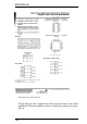
PadName
EAGLE automatically assigns pad names, P$1, P$2, P$3 etc., as place
-
ment proceeds. Assign the names in accordance with the information in
thedatabook.
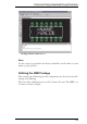
The names can be checked easily by clicking the Options/Set/Misc menu
and choosing the Display pad names option. All pad names are displayed
afterrefreshingthescreen(F2).
Alternativelytypeinthecommandline:
SETPADON
Tohidethepadnamesagain:
SETPADOFF
The following procedure is recommended for components that have a
largenumberofsequentiallynumberedpads:
Select the PAD command, type in the name of the first pad, e.g. '1', and
place the pads in sequence. The single quote marks must be typed on the
command line. See also the section on Names and Automatic Naming on
page 73.
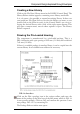
DrawtheSilkScreenSymbol
A simple silk screen symbol that is to be visible on the board is drawn in
layer 21, tPlace. Use the commands WIRE, CIRCLE, and ARC. Ensure
that it does not cover soldered areas, since this can cause problems when
the boards come to be soldered. If necessary, use the GRID command
to set a finer grid or use the Alt key for the alternative grid (see GRID
command). The standard width (CHANGE WIDTH) for lines in the
screenprintis10mil(0.254mm),andshouldnotbemadethinner.
It is also possible to create an additional and rather better-looking silk
screen for documentation purposes in layer 51, tDocu. This may indeed
cover soldered areas, since it is not output along with the manufacturing
data.
PackageNameandPackageValue
Thelabelingnowfollows.UsetheTEXTcommandandwrite
>NAME
inlayer25, tNames,forthenameplaceholder,and
>VALUE
171
ComponentDesignExplainedthroughExamples