
User Guide

Example—Creating a Hierarchical Design
247
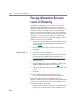
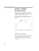
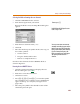
Wiring the Symbols
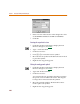
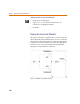
Now that you have placed all of the symbols, wire the
symbols to look like the schematic shown in Figure 20.
1 Click the Draw Wire button to change the pointer to a
pencil.
2 Click the top of V1. Click at the location of the wire
vertex (where it turns from the vertical to the
horizontal). Click the left side of the CMOS block. The
wire is complete when it shows connection on both
ends.
3 Repeat step 2 to connect a wire from the right side of
the CMOS block to the top of the load resistor.
4 Right-click to stop wire drawing.
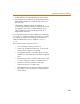
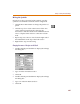
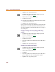
Changing the names of the pins on the block
1 Double-click the pin labeled P1 to display the Change
Pin dialog box.
2 Type
IN in the Pin Name text box.
3 Click OK.
4 Double-click the pin labeled P2 to display the Change
Pin dialog box.
5 Type
OUT in the Pin Name text box.
6 Click OK.