
User`s manual
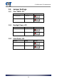

CT-XBT0x Mini-ITX Motherboard
28
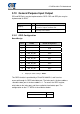
3.10 General Purpose Input Output
GPI and GPO pins may be implemented as GPIO. GPI and GPO pins may be
implemented as SDIO.
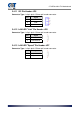
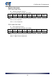
Signal I/O Description
GPO[0:3] O
General purpose output pins. Upon a hardware
reset, these outputs should be low.
GPI[0:3] I
General purpose input pins. Pulled high
internally on the Module.
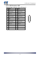
3.10.1 GPIO Configuration
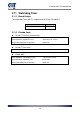
Board Design
Pin# GPIO# Default Configuration
1 VCC3
2 GND
3 DIO_PH_OUT0 GPO0
4 DIO_PH_IN0 GPI0
5 DIO_PH_OUT1 GPO1
6 DIO_PH_IN1 GPI1
7 DIO_PH_OUT2 GPO2
8 DIO_PH_IN2 GPI2
9 DIO_PH_OUT3 GPO3
10 DIO_PH_IN3 GPI3
Notes
1. Output pin default setting is “HIGH”
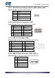
The GPIO function is provided by a Fintek F81866 AD-I, and it can be
accessed through its GPIO index/data port. The index port is the base address
+0 and the data port is the base address +1. To access the GPIO register,
write index to the index port, and then read/write from/to data port. The
configuration on the CT- XBT0x is described as below.
Index Port 0xA00
Data Port 0xA01