
Owner's manual


VSKDS201/045
www.vishay.com
Vishay Semiconductors
Revision: 04-Jan12
4
Document Number: 93234
For technical questions within your region: DiodesAmericas@vishay.com
, DiodesAsia@vishay.com, DiodesEurope@vishay.com
THIS DOCUMENT IS SUBJECT TO CHANGE WITHOUT NOTICE. THE PRODUCTS DESCRIBED HEREIN AND THIS DOCUMENT
ARE SUBJECT TO SPECIFIC DISCLAIMERS, SET FORTH AT www.vishay.com/doc?91000
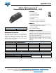
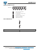
Fig. 5 - Maximum Allowable Case Temperature vs.
Average Forward Current
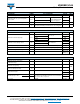
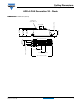
Fig. 6 - Forward Power Loss Characteristics
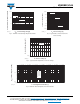
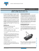
Fig. 7 - Maximum Non-Repetitive Surge Current
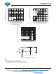
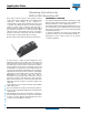
Fig. 8 - Unclamped Inductive Test Circuit
Note
(1)
Formula used: T
C
= T
J
- (Pd + Pd
REV
) x R
thJC
;
Pd = Forward power loss = I
F(AV)
x V
FM
at (I
F(AV)
/D) (see fig. 6);
Pd
REV
= Inverse power loss = V
R1
x I
R
(1 - D); I
R
at V
R1
= 80 % rated V
R
Allowable Case Temperature (°C)
I
F(AV)
- Average Forward Current (A)
20015010050 250
300
0
80
140
180
0
40
60
100
160
120
20
93234_05
Square wave (D = 0.50)
Rated V
R
applied
See note (1)
DC
Average Power Loss (W)
I
F(AV)
- Average Forward Current (A)
80 120100 140604020
160
0
93234_06
80
100
120
0
40
60
20
D = 0.75
D = 0.20
D = 0.25
D = 0.33
D = 0.50
RMS limit
DC
1000
10 100
t
p
- Square Wave Pulse Duration (µs)
I
FSM
- Non-Repetitive Surge Current (A)
93234_07
1000 10 000
10 000
At any rated load condition
and with rated V
RRM
applied
following surge
Current
monitor
High-speed
switch
D.U.T.
R
g
= 25 Ω
+
Freewheel
diode
V
d
= 25 V
L
IRFP460
40HFL40S02