6121 Baker Road, Suite 108 Minnetonka, MN 55345 Phone (952) 933-6190 Fax (952) 933-6223 1-800-274-4284 www.chtechnology.com Thank you for downloading this document from C&H Technology, Inc. Please contact the C&H Technology team for the following questions Technical ● Application ● Assembly ● Availability ● Pricing Phone – 1-800-274-4284 E-Mail – sales@chtechnology.com www.chtechnology.com - SPECIALISTS IN POWER ELECTRONIC COMPONENTS AND ASSEMBLIES - www.chtechnology.
VSKCS220/030 www.vishay.
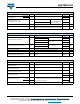
VSKCS220/030 www.vishay.com Vishay Semiconductors ABSOLUTE MAXIMUM RATINGS PARAMETER Maximum average forward current per module per leg SYMBOL TEST CONDITIONS IF(AV) 50 % duty cycle at TC = 110 °C, rectangular waveform 5 μs sine or 3 μs rect.
VSKCS220/030 Vishay Semiconductors 1000 10 000 IR - Reverse Current (mA) IF - Instantaneous Forward Current (A) www.vishay.com 100 TJ = 150 °C 10 TJ = 125 °C TJ = 25 °C 1 0.0 1000 150 °C 125 °C 100 100 °C 75 °C 10 50 °C 1 25 °C 0.1 0.01 0.3 0.6 0.9 1.2 0 1.5 5 10 15 20 25 30 VR - Reverse Voltage (V) VFM - Forward Voltage Drop (V) Fig. 1 - Maximum Forward Voltage Drop Characteristics Fig. 2 - Typical Values of Reverse Current vs.
VSKCS220/030 Vishay Semiconductors 100 160 Square wave (D = 0.50) 80 % rated VR applied 140 Average Power Loss (W) Allowable Case Temperature (°C) www.vishay.com 120 100 DC 80 60 40 20 80 D = 0.75 D = 0.50 D = 0.33 D = 0.25 D = 0.20 60 RMS limit 40 20 DC see note (1) 0 0 0 50 100 150 200 250 0 300 40 60 80 100 120 140 160 180 IF(AV) - Average Forward Current (A) IF(AV) - Average Forward Current (A) Fig. 6 - Forward Power Loss Characteristics Fig.
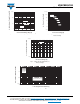
VSKCS220/030 www.vishay.com Vishay Semiconductors ORDERING INFORMATION TABLE Device code VS KC S 22 0 1 2 3 4 5 / 1 - Vishay Semiconductors product 2 - Circuit configuration: 030 6 KC = ADD-A-PAK - 2 diodes/common cathode 3 - S = Schottky diode 4 - Average rating (x 10) 5 - Product silicon identification 6 - Voltage rating (030 = 30 V) CIRCUIT CONFIGURATION (1) + (2) - (3) - LINKS TO RELATED DOCUMENTS Dimensions Revision: 04-Jan-12 www.vishay.
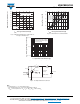
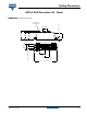
Outline Dimensions Vishay Semiconductors ADD-A-PAK Generation VII - Diode DIMENSIONS in millimeters (inches) 29 ± 0.5 (1 ± 0.020) 30 ± 0.5 (1.18 ± 0.020) 35 REF. 18 (0.7) REF. 24 ± 0.5 (1 ± 0.020) 6.7 ± 0.3 (0.26 ± 0.012) Viti M5 x 0.8 Screws M5 x 0.8 Document Number: 95369 Revision: 11-Nov-08 7 6 4 5 3 2 1 6.3 ± 0.2 (0.248 ± 0.008) 22.6 ± 0.2 (0.89 ± 0.008) 80 ± 0.3 (3.15 ± 0.012) 15 ± 0.5 (0.59 ± 0.020) 20 ± 0.5 (0.79 ± 0.020) 20 ± 0.5 (0.79 ± 0.020) 92 ± 0.75 (3.6 ± 0.
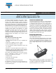
VISHAY SEMICONDUCTORS Modules Application Note Mounting Instructions for ADD-A-PAK Generation VII Generation VII ADD-A-PAK (AAP) power modules combine the excellent thermal performance enabled by a direct bonded copper (Al2O3) substrate, superior mechanical ruggedness, and an environmentally friendly manufacturing process that eliminates the use of hard molds, thus reducing direct stresses on the leads. To prevent axial pull-out, the electrical terminals are co-molded to the module housing.
Application Note Vishay Semiconductors Mounting Instructions for ADD-A-PAK Generation VII Next, make a uniform coating on the heatsink mounting surfaces and module substrate with a good quality thermal compound. Screen printing of the compound is recommended, as well as direct application through a roller or spatula. The datasheet values for thermal resistance assume a uniform layer of thermal compound with a maximum thickness of 0.08 mm. The thermal conductivity of the compound should be no less than 0.
Legal Disclaimer Notice www.vishay.com Vishay Disclaimer ALL PRODUCT, PRODUCT SPECIFICATIONS AND DATA ARE SUBJECT TO CHANGE WITHOUT NOTICE TO IMPROVE RELIABILITY, FUNCTION OR DESIGN OR OTHERWISE. Vishay Intertechnology, Inc., its affiliates, agents, and employees, and all persons acting on its or their behalf (collectively, “Vishay”), disclaim any and all liability for any errors, inaccuracies or incompleteness contained in any datasheet or in any other disclosure relating to any product.