6121 Baker Road, Suite 108 Minnetonka, MN 55345 Phone (952) 933-6190 Fax (952) 933-6223 1-800-274-4284 www.chtechnology.com Thank you for downloading this document from C&H Technology, Inc. Please contact the C&H Technology team for the following questions - Technical Application Assembly Availability Pricing Phone – 1-800-274-4284 E-Mail – sales@chtechnology.com www.chtechnology.com - SPECIALISTS IN POWER ELECTRONIC COMPONENTS AND ASSEMBLIES - www.chtechnology.
VSK.71, .91..
VSK.71, .91..
VSK.71, .91..PbF Series Thyristor/Diode and Thyristor/Thyristor Vishay High Power Products TM (ADD-A-PAK Generation 5 Power Modules), 75/95 A TRIGGERING PARAMETER SYMBOL Maximum peak gate power Maximum average gate power VSK.71 VSK.91 PGM 12 PG(AV) 3.0 IGM 3.0 - VGM 10 Maximum peak gate current Maximum peak negative gate voltage TEST CONDITIONS Maximum gate voltage required to trigger VGT Anode supply = 6 V resistive load TJ = 25 °C V 1.7 270 TJ = - 40 °C IGT A 2.
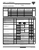
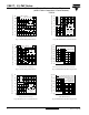
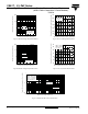
VSK.71, .91..PbF Series Maximum Allowable Case Temperature (°C) 130 VSK.71.. Series RthJC (DC) = 0.33 K/ W 120 110 Cond uction Angle 100 90 30° 60° 90° 80 120° 180° 70 0 10 20 30 40 50 60 70 80 Maximum Average On-state Power Loss (W) Thyristor/Diode and Thyristor/Thyristor (ADD-A-PAKTM Generation 5 Power Modules), 75/95 A Vishay High Power Products 140 DC 180° 120° 90° 60° 30° 120 100 80 RMS Limit 60 Conduction Period 40 VSK.71.. Series Per Junction TJ = 125°C 20 0 0 20 VSK.71..
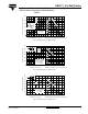
VSK.71, .91..PbF Series Thyristor/Diode and Thyristor/Thyristor Vishay High Power Products TM (ADD-A-PAK Generation 5 Power Modules), 75/95 A = 0. /W 1K W K/ 0. 4 W K/ 3 0. 200 SA R th 180° 120° 90° 60° 30° 2 0. K/ W 0. 5 K/ W 0.7 K/ W 150 ta el -D R Maximum Total On-sta te Power Lo ss (W) 250 1K /W 100 Conduction Angle 1.5 K/ W VSK.71..
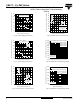
VSK.71, .91..PbF Series VSK.91.. Series RthJC (DC) = 0.27 K/ W 120 110 Cond uc tion Angle 100 90 30° 60° 90° 120° 80 180° 70 0 20 40 60 80 100 Maximum Average On-state Power Loss (W) 130 Thyristor/Diode and Thyristor/Thyristor (ADD-A-PAKTM Generation 5 Power Modules), 75/95 A DC 180° 120° 90° 60° 30° 160 140 120 100 RMS Limit 80 Conduction Period 60 VSK.91.. Series Per Junc tion TJ = 125°C 40 20 0 0 20 40 60 80 100 120 140 160 Average On-state Current (A) Fig.
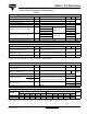
VSK.71, .91..PbF Series Thyristor/Diode and Thyristor/Thyristor Vishay High Power Products TM (ADD-A-PAK Generation 5 Power Modules), 75/95 A VSK.91.. Series Per Mod ule TJ = 125°C 50 0. 5K /W 0.7 K/ W 1K /W 1.5 K /W R 100 a Conduc tion Angle K/ W e lt -D 150 K/ W W K/ 200 0. 3 1 0. 250 0.
VSK.71, .91..PbF Series Thyristor/Diode and Thyristor/Thyristor (ADD-A-PAKTM Generation 5 Power Modules), 75/95 A Maximum Reverse Rec overy Cha rge - Qrr (µC) Vishay High Power Products Instantaneous On-state Current (A) 1000 100 TJ= 25°C 10 TJ= 125°C VSK.71.. Series Per Junction 1 0.5 1 1.5 2 2.5 3 3.5 4 700 50 A 400 100 10 Maximum Reverse Re covery Current - Irr (A) Instantaneous On-state Current (A) TJ= 25°C TJ= 125°C VSK.91.. Series Per Junction 2 2.
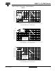
VSK.71, .91..PbF Series Thyristor/Diode and Thyristor/Thyristor Vishay High Power Products TM (ADD-A-PAK Generation 5 Power Modules), 75/95 A Rectangular gate pulse a)Recommended load line for rated di/ dt: 20 V, 20 ohms tr = 0.
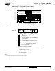
VSK.71, .91..PbF Series Thyristor/Diode and Thyristor/Thyristor (ADD-A-PAKTM Generation 5 Power Modules), 75/95 A Vishay High Power Products CIRCUIT CONFIGURATION VSKH VSKT (1) (1) ~ 2 + (2) + (2) 3 (3) G1 K1 K2 G2 (4) (5) (7) (6) - 1 + (2) 2 2 + (2) 3 3 4 5 4 5 76 (1) ~ 1 2 3 (1) ~ 1 1 VSKN VSKL 4 5 76 (3) K2 G2 (7) (6) (3) G1 K1 (4) (5) + (3) G1 K1 (4) (5) LINKS TO RELATED DOCUMENTS Dimensions www.vishay.com 10 http://www.vishay.