6121 Baker Road, Suite 108 Minnetonka, MN 55345 Phone (952) 933-6190 Fax (952) 933-6223 1-800-274-4284 www.chtechnology.com Thank you for downloading this document from C&H Technology, Inc. Please contact the C&H Technology team for the following questions - Technical Application Assembly Availability Pricing Phone – 1-800-274-4284 E-Mail – sales@chtechnology.com www.chtechnology.com - SPECIALISTS IN POWER ELECTRONIC COMPONENTS AND ASSEMBLIES - www.chtechnology.
VSK.71..
VSK.71..
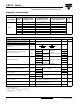
VSK.71.. Series ADD-A-PAK Generation VII Power Modules Vishay High Power Products Thyristor/Diode and Thyristor/Thyristor, 75 A TRIGGERING PARAMETER SYMBOL PGM 12 3.0 IGM 3.0 Maximum peak gate current Maximum peak negative gate voltage VALUES PG(AV) Maximum peak gate power Maximum average gate power TEST CONDITIONS - VGM VGT W A 10 TJ = - 40 °C Maximum gate voltage required to trigger UNITS 4.0 Anode supply = 6 V resistive load TJ = 25 °C V 2.5 TJ = 125 °C 1.
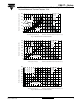
VSK.71.. Series ADD-A-PAK Generation VII Power Modules Thyristor/Diode and Thyristor/Thyristor, 75 A RthJC (DC) = 0.29°C/W 120 110 100 90 180° 120° 90° 60° 30° 80 70 0 Maximum allowable case temperature (°C) Maximum average on-state power loss (W) 130 10 20 30 40 50 60 70 180° 120° 90° 60° 30° 160 140 120 100 DC RMS limit 80 60 40 20 Per leg, Tj = 125°C 0 80 0 20 60 80 100 120 Fig. 1 - Current Ratings Characteristics Fig.
VSK.71.. Series ADD-A-PAK Generation VII Power Modules Vishay High Power Products Thyristor/Diode and Thyristor/Thyristor, 75 A Maximum total on-state power loss (W) 300 RthSA = 0.1 °C/W 0.2 °C/W 0.3 °C/W 0.4 °C/W 0.5 °C/W 0.7 °C/W 1 °C/W 1.5 °C/W 3 °C/W 180° 120° 90° 60° 30° 250 200 150 100 VSK.71 Series Per module Tj = 125°C 50 0 0 20 40 60 80 100 120 140 160 180 0 20 Total RMS output current (A) 40 60 80 100 120 140 Maximum allowable ambient temperature (°C) Fig.
VSK.71.. Series ADD-A-PAK Generation VII Power Modules Thyristor/Diode and Thyristor/Thyristor, 75 A Vishay High Power Products Instantaneous on-state current (A) 1000 Per leg 100 10 Tj = 125°C Tj = 25°C 1 0.5 1.0 1.5 2.0 2.5 3.0 3.5 Instantaneous on-state voltage (V) Transient thermal impedance Z thJC (°C/W) Fig. 10 - On-State Voltage Drop Characteristics 1 Steady state value RthJC = 0.29 °C/W (DC operation) 0.1 Per leg 0.01 0.001 0.01 0.1 1 10 Square wave pulse duration (s) Fig.
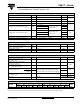
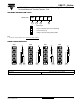
VSK.71.. Series ADD-A-PAK Generation VII Power Modules Vishay High Power Products Thyristor/Diode and Thyristor/Thyristor, 75 A ORDERING INFORMATION TABLE Device code VSK T 71 1 2 3 / 16 4 1 - Module type 2 - Circuit configuration (see end of datasheet) 3 - Current code (75 A) 4 - Voltage code (see Voltage Ratings table) Note • To order the optional hardware go to www.vishay.
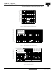
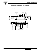
Outline Dimensions Vishay High Power Products ADD-A-PAK Generation VII - Thyristor DIMENSIONS in millimeters (inches) 29 ± 0.5 (1 ± 0.020) 30 ± 0.5 (1.18 ± 0.020) 35 REF. 18 (0.7) REF. 30 ± 1 (1.18 ± 0.039) 15.5 ± 0.5 (0.6 ± 0.020) 24 ± 0.5 (1 ± 0.020) Viti M5 x 0.8 Screws M5 x 0.8 6.7 ± 0.3 (0.26 ± 0.012) Fast-on tab 2.8 x 0.8 (0.110 x 0.03) Document Number: 95368 Revision: 11-Nov-08 20 ± 0.5 (0.79 ± 0.020) 20 ± 0.5 (0.79 ± 0.020) 92 ± 0.75 (3.6 ± 0.030) 5.8 ± 0.25 (0.228 ± 0.010) 15 ± 0.
V I S H AY H I G H POW E R P R O D U C T S Modules Application Note Mounting Instructions for ADD-A-PAK Generation VII Generation VII ADD-A-PAK (AAP) power modules combine the excellent thermal performance enabled by a direct bonded copper (Al2O3) substrate, superior mechanical ruggedness, and an environmentally friendly manufacturing process that eliminates the use of hard molds, thus reducing direct stresses on the leads.
Application Note Vishay High Power Products Mounting Instructions for ADD-A-PAK Generation VII Next, make a uniform coating on the heatsink mounting surfaces and module substrate with a good quality thermal compound. Screen printing of the compound is recommended, as well as direct application through a roller or spatula. The datasheet values for thermal resistance assume a uniform layer of thermal compound with a maximum thickness of 0.08 mm.