
Owner manual

Document Number: 00266x For technical questions, contact: ind-modules@vishay.com
www.vishay.com
Revision: 05-May-09 3
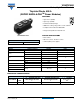
VSHPS1480
Thyristor/Diode, 500 A
(SUPER MAGN-A-PAK
TM
Power Modules)
Vishay High Power Products
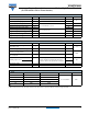
Note
• Table shows the increment of thermal resistance R
thJC
when devices operate at different conduction angles than DC
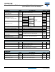
TRIGGERING
PARAMETER SYMBOL TEST CONDITIONS VALUES UNITS
Maximum peak gate power P
GM
T
J
= T
J
maximum, t
p
≤ 5 ms 10
W
Maximum peak average gate power P
G(AV)
T
J
= T
J
maximum, f = 50 Hz, d% = 50 2.0
Maximum peak positive gate current +I
GM
T
J
= T
J
maximum, t
p
≤ 5 ms
3.0 A
Maximum peak positive gate voltage +V
GM
20
V
Maximum peak negative gate voltage -V
GM
5.0
Maximum DC gate current required to trigger I
GT
T
J
= 25 °C, V
ak
12 V
200 mA
DC gate voltage required to trigger V
GT
3.0 V
DC gate current not to trigger I
GD
T
J
= T
J
maximum 10 mA
DC gate voltage not to trigger V
GD
0.25 V
THERMAL AND MECHANICAL SPECIFICATIONS
PARAMETER SYMBOL TEST CONDITIONS VALUES UNITS
Maximum junction operating
temperature range
T
J
- 40 to 130
°C
Maximum storage temperature range T
Stg
- 40 to 150
Maximum thermal resistance,
junction to case per junction
R
thJC
DC operation 0.065
K/W
Maximum thermal resistance,
case to heatsink
R
thC-hs
0.02
Mounting torque ± 10 %
SMAP to heatsink
A mounting compound is recommended and the
torque should be rechecked after a period of
3 hours to allow for the spread of the compound.
6-8
Nm
busbar to SMAP 12-15
Approximate weight 1500 g
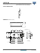
Case style See dimensions SUPER MAGN-A-PAK
ΔR
thJC
CONDUCTION
CONDUCTION ANGLE SINUSOIDAL CONDUCTION RECTANGULAR CONDUCTION TEST CONDITIONS UNITS
180° 0.009 0.006
T
J
= T
J
maximum K/W
120° 0.011 0.011
90° 0.014 0.015
60° 0.021 0.022
30° 0.037 0.038