
User Manual
Document Number: 93882 For technical questions, contact: die-wafer@vishay.com
www.vishay.com
Revision: 28-Mar-08 1
Fast Recovery Diodes
VS180LM..CS02CB Series
Vishay High Power Products
FEATURES
• 100 % tested at probe
• Bondable top metal
• Wafer in box, and die in chip carrier
Note
(1)
Nitrogen flow on die edge
ORDERING INFORMATION TABLE
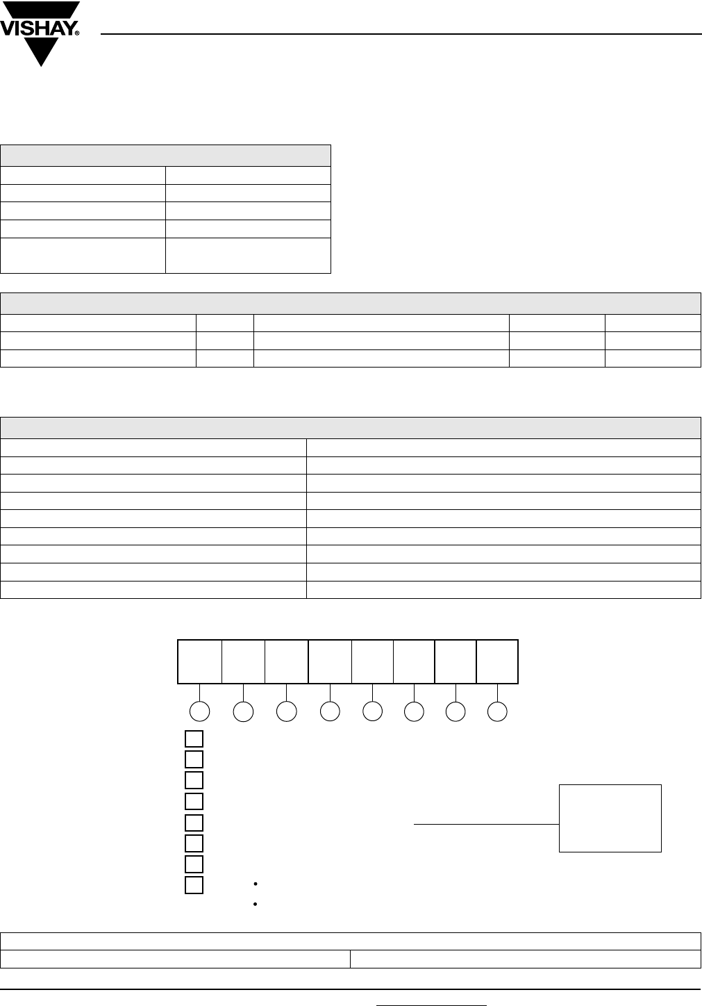
PRODUCT SUMMARY
Junction size Square 180 mils
Wafer size 4"
V
RRM
class 200 to 600 V
Passivation process Glassivated MOAT
Reference Vishay HPP
packaged part
20ETF Series
RoHS
COMPLIANT
MAJOR RATINGS AND CHARACTERISTICS
PARAMETER SYMBOL TEST CONDITIONS VALUES UNITS
Maximum forward voltage V
FM
T
J
= 25 °C, I
F
= 20 A 1300 mV
Maximum repetitive reverse voltage V
RRM
(1)
T
J
= 25 °C, I
RRM
= 100 µA 200 to 600 V
MECHANICAL DATA
Nominal back metal composition (thickness) Cr-Ni-Ag (1 kÅ - 4 kÅ - 6 kÅ)
Nominal front metal composition (thickness) 100 % Al (20 µm)
Chip dimensions 180 x 180 mils (4.57 x 4.57) - see dimensions (link at the end of datasheet)
Wafer diameter 100 mm, with standard < 110 > flat
Wafer thickness 260 µm
Maximum width of sawing line 45 µm
Reject ink dot size Ø 0.25 mm minimum
Ink dot location See dimensions (link at the end of datasheet)
Recommended storage environment Storage in original container, in desiccated nitrogen, with no contamination
Device code
1 - Vishay HPP device
2 - Chip dimension in mils
3 - Type of device: L = Wire bondable fast recovery diode
4 - Passivation process: M = Glassivated MOAT
5 - Voltage code x 100 = V
RRM
6
- Metallization: C = Aluminum (anode) - silver (cathode)
7 -t
rr
code: S02 = 200 ns
8 - CB = Probed uncut die (wafer in box)
None = Probed die in chip carrier
Available class
02 = 200 V
04 = 400 V
06 = 600 V
51324678
VS 180 L M 06 C S02 CB
LINKS TO RELATED DOCUMENTS
Dimensions http://www.vishay.com/doc?95153