6121 Baker Road, Suite 108 Minnetonka, MN 55345 Phone (952) 933-6190 Fax (952) 933-6223 1-800-274-4284 www.chtechnology.com Thank you for downloading this document from C&H Technology, Inc. Please contact the C&H Technology team for the following questions - Technical Application Assembly Availability Pricing Phone – 1-800-274-4284 E-Mail – sales@chtechnology.com www.chtechnology.com - SPECIALISTS IN POWER ELECTRONIC COMPONENTS AND ASSEMBLIES - www.chtechnology.
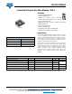
VS-UFL230FA60 www.vishay.com Vishay Semiconductors Insulated Ultrafast Rectifier Module, 230 A FEATURES • Two fully independent diodes • Fully insulated package • Ultrafast, soft reverse recovery, with high operation junction temperature (TJ max.
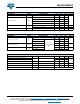
VS-UFL230FA60 www.vishay.com Vishay Semiconductors ELECTRICAL SPECIFICATIONS PER DIODE (TJ = 25 °C unless otherwise specified) PARAMETER Cathode to anode breakdown voltage Forward voltage SYMBOL VBR VFM Reverse leakage current IRM Junction capacitance CT TEST CONDITIONS IR = 100 μA MIN. TYP. MAX. 600 - - IF = 100 A - 1.28 1.44 IF = 100 A, TJ = 125 °C - 1.13 1.24 IF = 200 A - 1.48 1.66 UNITS V IF = 200 A, TJ = 125 °C - 1.37 1.55 VR = VR rated - 0.
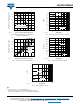
VS-UFL230FA60 Vishay Semiconductors 1000 1000 TJ = 175 °C IR - Reverse Current (mA) IF - Instantaneous Forward Current (A) www.vishay.com TJ = 175 °C 100 TJ = 125 °C 10 TJ = 25 °C 0.5 1 1.5 2 2.5 VFM - Forward Voltage Drop (V) 93635_01 10 TJ = 125 °C 1 0.1 0.01 0.001 0 1 0 100 100 200 300 400 500 600 VR - Reverse Voltage (V) 93635_02 Fig. 1 - Typical Forward Voltage Drop Characteristics TJ = 25 °C Fig. 2 - Typical Values of Reverse Current vs.
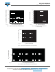
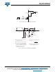
VS-UFL230FA60 www.vishay.com Vishay Semiconductors 250 230 150 TJ = 125 °C 210 125 190 100 trr (ns) Allowable Case Temperature (°C) 175 DC 75 170 150 130 110 50 Square wave (D = 0.50) 80 % Rated VR applied 25 90 TJ = 25 °C 70 0 50 0 40 80 120 160 200 240 100 280 IF(AV) - Average Forward Current (A) 93635_05 1000 dIF/dt (A/µs) 93635_07 Fig. 7 - Typical Reverse Recovery Time vs. dIF/dt Fig. 5 - Maximum Allowable Case Temperature vs.
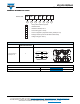
VS-UFL230FA60 www.vishay.com Vishay Semiconductors VR = 200 V 0.01 Ω L = 70 μH D.U.T. dIF/dt adjust D IRFP250 G S Fig. 10 - Reverse Recovery Parameter Test Circuit (3) trr IF ta tb 0 Qrr (2) IRRM (4) 0.5 IRRM dI(rec)M/dt (5) 0.75 IRRM (1) dIF/dt (1) dIF/dt - rate of change of current through zero crossing (2) IRRM - peak reverse recovery current (3) trr - reverse recovery time measured from zero crossing point of negative going IF to point where a line passing through 0.75 IRRM and 0.
VS-UFL230FA60 www.vishay.
Legal Disclaimer Notice www.vishay.com Vishay Disclaimer ALL PRODUCT, PRODUCT SPECIFICATIONS AND DATA ARE SUBJECT TO CHANGE WITHOUT NOTICE TO IMPROVE RELIABILITY, FUNCTION OR DESIGN OR OTHERWISE. Vishay Intertechnology, Inc., its affiliates, agents, and employees, and all persons acting on its or their behalf (collectively, “Vishay”), disclaim any and all liability for any errors, inaccuracies or incompleteness contained in any datasheet or in any other disclosure relating to any product.