
Manual

VS-HFA70FA120
www.vishay.com
Vishay Semiconductors
Revision: 29-Feb-12
5
Document Number: 94289
For technical questions within your region: DiodesAmericas@vishay.com
, DiodesAsia@vishay.com, DiodesEurope@vishay.com
THIS DOCUMENT IS SUBJECT TO CHANGE WITHOUT NOTICE. THE PRODUCTS DESCRIBED HEREIN AND THIS DOCUMENT
ARE SUBJECT TO SPECIFIC DISCLAIMERS, SET FORTH AT www.vishay.com/doc?91000
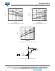
Fig. 11 - Reverse Recovery Waveform and Definitions
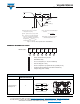
ORDERING INFORMATION TABLE
CIRCUIT CONFIGURATION
CIRCUIT
CIRCUIT
CONFIGURATION CODE
CIRCUIT DRAWING
2 separate diodes,
parallel pin-out
F
Q
rr
0.5 I
RRM
dI
(rec)M
/dt
0.75 I
RRM
I
RRM
t
rr
t
b
t
a
I
F
dI
F
/dt
0
(1)
(2)
(3)
(4)
(5)
(1) dI
F
/dt - rate of change of current
through zero crossing
(2) I
RRM
- peak reverse recovery current
(3) t
rr
- reverse recovery time measured
from zero crossing point of negative
going I
F
to point where a line passing
through 0.75 I
RRM
and 0.50 I
RRM
extrapolated to zero current.
(4) Q
rr
- area under curve dened by t
rr
and I
RRM
t
rr
x I
RRM
2
Q
rr
=
(5) dI
(rec)M
/dt - peak rate of change of
current during t
b
portion of t
rr
1 -Vishay Semiconductors product
2 - HEXFRED
®
family
3
- Process designator (A = electron irradiated)
4 - Current rating (70 = 70 A)
5 - Circuit conguration (2 separate diodes, parallel pin-out)
6 - Package indicator (SOT-227 standard isolated base)
- Voltage rating (120 = 1200 V)
7
Device code
51 32 4 6 7
VS- HF A 70 F A 120
1
43
2
Lead Assignment
1
4
2
3