
Manual

VS-HFA70FA120
www.vishay.com
Vishay Semiconductors
Revision: 29-Feb-12
3
Document Number: 94289
For technical questions within your region: DiodesAmericas@vishay.com
, DiodesAsia@vishay.com, DiodesEurope@vishay.com
THIS DOCUMENT IS SUBJECT TO CHANGE WITHOUT NOTICE. THE PRODUCTS DESCRIBED HEREIN AND THIS DOCUMENT
ARE SUBJECT TO SPECIFIC DISCLAIMERS, SET FORTH AT www.vishay.com/doc?91000
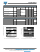
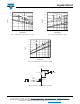
Fig. 3 - Typical Junction Capacitance vs. Reverse Voltage
Fig. 4 - Maximum Thermal Impedance Z
thJC
Characteristics (Per Leg)
Fig. 5 - Maximum Allowable Case Temperature
vs. Average Forward Current (Per Leg)
Fig. 6 - Forward Power Losses Characteristics (Per Leg)
10
100
1000
10 100 1000 10 000
C
T
- Junction Capacitance (pF)
V
R
- Reverse Voltage (V)
0.001
0.01
0.1
1
0.0001 0.001 0.01 0.1 1
t
1
- Rectangular Pulse Duration (s)
Z
thJC
- Thermal Impedance (°C/W)
Single pulse
(thermal resistance)
.
.
P
DM
t
1
t
2
Notes:
1. Duty factor D = t
1
/t
2
2. Peak T
J
= P
DM
x Z
thJC
+ T
C
D = 0.75
D = 0.50
D = 0.33
D = 0.25
D = 0.20
DC
10
0
25
50
75
100
125
150
175
0 102030405060708090
Allowable Case Temperature (°C)
I
F
- Average Forward Current (A)
Square wave (d = 0.5)
80 % rated V
R
applied
DC
0
50
100
150
200
0 10203040506070
Average Power Loss (W)
I
F(AV)
- Average Forward Current (A)
DC
D = 0.20
D = 0.25
D = 0.33
D = 0.50
D = 0.75
RMS Limit