6121 Baker Road, Suite 108 Minnetonka, MN 55345 Phone (952) 933-6190 Fax (952) 933-6223 1-800-274-4284 www.chtechnology.com Thank you for downloading this document from C&H Technology, Inc. Please contact the C&H Technology team for the following questions - Technical Application Assembly Availability Pricing Phone – 1-800-274-4284 E-Mail – sales@chtechnology.com www.chtechnology.com - SPECIALISTS IN POWER ELECTRONIC COMPONENTS AND ASSEMBLIES - www.chtechnology.
VS-GT400TH60N www.vishay.
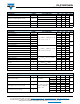
VS-GT400TH60N www.vishay.com Vishay Semiconductors IGBT ELECTRICAL SPECIFICATIONS (TC = 25 °C unless otherwise noted) PARAMETER Collector to emitter breakdown voltage SYMBOL V(BR)CES TEST CONDITIONS VGE = 0 V, IC = 2 mA, TJ = 25 °C MIN. TYP. MAX. 600 - - VGE = 15 V, IC = 400 A, TJ = 25 °C - 1.6 2.05 VGE = 15 V, IC = 400 A, TJ = 175 °C - 2.0 6.5 UNITS Collector to emitter saturation voltage VCE(on) V Gate to emitter threshold voltage VGE(th) VCE = VGE, IC = 4 mA, TJ = 25 °C 4.
VS-GT400TH60N www.vishay.com Vishay Semiconductors THERMAL AND MECHANICAL SPECIFICATIONS PARAMETER SYMBOL MIN. TYP. MAX. TJ - - 175 TStg - 40 - 125 - - 0.094 - - 0.158 - 0.035 - Operating junction temperature range Storage temperature range TEST CONDITIONS °C IGBT Junction to case per ½ module RthJC Diode Case to sink RthCS Conductive grease applied Power terminal screw: M6 2.5 to 5.0 Mounting screw: M6 3.0 to 5.
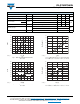
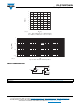
VS-GT400TH60N www.vishay.com Vishay Semiconductors 900 800 IC, module 700 IC (A) 600 500 400 300 200 100 0 0 93488_05 100 200 300 400 500 600 700 VCE (V) Fig. 5 - RBSOA Rg = 1.3 , VGE = ± 15 V, TJ = 175 °C ZthJC (K/W) 1 0.1 IGBT 0.01 0.001 0.001 0.01 0.1 1 10 t (s) Fig. 6 - IGBT Transient Thermal Impedance 93488_06 12 800 700 10 600 8 E (mJ) IC (A) 500 400 300 Erec 6 4 200 150 °C 2 25 °C 100 0 0 0 0.5 1.0 1.5 2.0 VF (V) 93488_07 Fig.
VS-GT400TH60N www.vishay.com Vishay Semiconductors 8 7 6 Erec E (mJ) 5 4 3 2 1 0 0 2 4 6 8 10 12 Rg (Ω) 93488_09 Fig. 9 - Diode Switching Loss vs. Gate Resistance VCC = 600 V, IC = 400 A, VGE = - 15 V, TJ = 125 °C ZthJC (K/W) 1 0.1 Diode 0.01 0.001 0.001 93488_10 0.01 0.1 1 10 t (s) Fig. 10 - Diode Transient Thermal Impedance CIRCUIT CONFIGURATION 6 7 1 2 3 5 4 LINKS TO RELATED DOCUMENTS Dimensions Revision: 06-Aug-12 www.vishay.
Legal Disclaimer Notice www.vishay.com Vishay Disclaimer ALL PRODUCT, PRODUCT SPECIFICATIONS AND DATA ARE SUBJECT TO CHANGE WITHOUT NOTICE TO IMPROVE RELIABILITY, FUNCTION OR DESIGN OR OTHERWISE. Vishay Intertechnology, Inc., its affiliates, agents, and employees, and all persons acting on its or their behalf (collectively, “Vishay”), disclaim any and all liability for any errors, inaccuracies or incompleteness contained in any datasheet or in any other disclosure relating to any product.