6121 Baker Road, Suite 108 Minnetonka, MN 55345 Phone (952) 933-6190 Fax (952) 933-6223 (800) 274-4284 Thank you for downloading this document from C&H Technology, Inc. Please contact the C&H Technology team for the following questions - Technical Application Assembly Availability Pricing Phone – 1-800-274-4284 E-Mail – sales@chtechnology.com C & H TECHNOLOGY, INC. ● 6121 BAKER RD. SUITE 108 ● MINNETONKA, MINNESOTA 55345 ● 800-274-4284 ● 952-933-6190 ● FAX: 952-933-6223 ● WWW.CHTECHNOLOGY.
VS-GT100DA120U www.vishay.
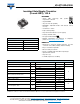
VS-GT100DA120U www.vishay.com Vishay Semiconductors ELECTRICAL SPECIFICATIONS (TJ = 25 °C unless otherwise specified) PARAMETER Collector to emitter breakdown voltage Collector to emitter voltage Gate threshold voltage Temperature coefficient of threshold voltage Collector to emitter leakage current Forward voltage drop Gate to emitter leakage current SYMBOL MIN. TYP. MAX. VGE = 0 V, IC = 250 μA 1200 - - VGE = 15 V, IC = 100 A - 1.73 2.1 VGE = 15 V, IC = 100 A, TJ = 125 °C - 1.98 2.2 4.
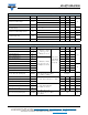
VS-GT100DA120U www.vishay.com Vishay Semiconductors THERMAL AND MECHANICAL SPECIFICATIONS PARAMETER SYMBOL Junction and storage temperature range IGBT Junction to case TEST CONDITIONS TJ, TStg RthJC Diode Case to heatsink RthCS Flat, greased surface Weight Mounting torque MAX. UNITS - 150 °C - - 0.14 - - 0.71 - 0.1 - - 30 - g - - 1.
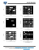
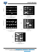
VS-GT100DA120U www.vishay.com Vishay Semiconductors 200 2.75 175 2.50 TJ = 150 °C 150 150 A 2.25 VCE (V) IF (A) 125 TJ = 25 °C 100 TJ = 125 °C 75 100 A 2.00 1.75 50 A 1.50 50 25 1.25 0 1.00 27 A 0 1 2 3 4 5 6 7 VFM (V) 93196_05 20 60 80 100 120 140 160 TJ (°C) 93196_08 Fig. 5 - Typical Diode Forward Characteristics Fig. 8 - Typical IGBT Collector to Emitter Voltage vs. Junction Temperature, VGE = 15 V 10 11 TJ = 150 °C 10 1 9 TJ = 125 °C 8 Energy (mJ) 0.
VS-GT100DA120U www.vishay.com Vishay Semiconductors 310 40 290 35 270 250 Energy (mJ) 30 230 trr (ns) 25 Eon 20 TJ = 125 °C 210 190 170 15 150 10 TJ = 25 °C 130 Eoff 110 5 0 10 20 30 40 90 100 50 Rg (Ω) 93196_11 1000 dIF/dt (A/μs) 93196_13 Fig. 13 - Typical trr Diode vs. dIF/dt Vrr = 400 V, IF = 50 A Fig. 11 - Typical IGBT Energy Loss vs.
VS-GT100DA120U www.vishay.com Vishay Semiconductors ZthJC - Thermal Impedance Junction to Case (°C/W) 1 0.1 D = 0.50 D = 0.20 D = 0.10 D = 0.05 D = 0.02 D = 0.01 DC 0.01 0.001 0.00001 0.0001 0.001 0.01 0.1 1 10 t1 - Rectangular Pulse Duration (s) 93196_16 Fig. 16 - Maximum Thermal Impedance ZthJC Characteristics (IGBT) ZthJC - Thermal Impedance Junction to Case (°C/W) 10 1 0.1 D = 0.50 D = 0.20 D = 0.10 D = 0.05 D = 0.02 D = 0.01 DC 0.01 0.001 0.00001 93196_17 0.0001 0.001 0.01 0.
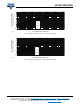
VS-GT100DA120U www.vishay.com Vishay Semiconductors R= L D.U.T. VCC ICM VC * 50 V 1000 V D.U.T. 1 2 + -V CC Rg * Driver same type as D.U.T.; VC = 80 % of Vce(max) * Note: Due to the 50 V power supply, pulse width and inductor will increase to obtain Id Fig. 18a - Clamped Inductive Load Test Circuit Fig. 18b - Pulsed Collector Current Test Circuit Diode clamp/ D.U.T. L - + -5V + VCC D.U.T./ driver Rg Fig.
VS-GT100DA120U www.vishay.
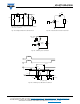
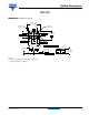
Outline Dimensions Vishay Semiconductors SOT-227 DIMENSIONS in millimeters (inches) 38.30 (1.508) 37.80 (1.488) Chamfer 2.00 (0.079) x 45° 4 x M4 nuts Ø 4.40 (0.173) Ø 4.20 (0.165) -A3 4 6.25 (0.246) 12.50 (0.492) 25.70 (1.012) 25.20 (0.992) -B- 1 2 R full 7.50 (0.295) 15.00 (0.590) 30.20 (1.189) 29.80 (1.173) 8.10 (0.319) 4x 7.70 (0.303) 2.10 (0.082) 1.90 (0.075) 0.25 (0.010) M C A M B M 2.10 (0.082) 1.90 (0.075) -C- 12.30 (0.484) 11.80 (0.464) 0.12 (0.
Legal Disclaimer Notice www.vishay.com Vishay Disclaimer ALL PRODUCT, PRODUCT SPECIFICATIONS AND DATA ARE SUBJECT TO CHANGE WITHOUT NOTICE TO IMPROVE RELIABILITY, FUNCTION OR DESIGN OR OTHERWISE. Vishay Intertechnology, Inc., its affiliates, agents, and employees, and all persons acting on its or their behalf (collectively, “Vishay”), disclaim any and all liability for any errors, inaccuracies or incompleteness contained in any datasheet or in any other disclosure relating to any product.