6121 Baker Road, Suite 108 Minnetonka, MN 55345 Phone (952) 933-6190 Fax (952) 933-6223 1-800-274-4284 www.chtechnology.com Thank you for downloading this document from C&H Technology, Inc. Please contact the C&H Technology team for the following questions - Technical Application Assembly Availability Pricing Phone – 1-800-274-4284 E-Mail – sales@chtechnology.com www.chtechnology.com - SPECIALISTS IN POWER ELECTRONIC COMPONENTS AND ASSEMBLIES - www.chtechnology.
VS-GB50NP120N www.vishay.com Vishay Semiconductors Molding Type Module IGBT, Chopper in 1 Package, 1200 V and 50 A FEATURES • • • • • High short circuit capability, self limiting to 6 x IC 10 μs short circuit capability Low inductance case Fast and soft reverse recovery antiparallel FWD Isolated copper baseplate using DCB (Direct Copper Bonding) technology • VCE(on) with positive temperature coefficient • Speed 8 kHz to 60 kHz • Material categorization: For definitions of compliance please see www.
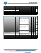
VS-GB50NP120N www.vishay.com Vishay Semiconductors IGBT ELECTRICAL SPECIFICATIONS (TC = 25 °C unless otherwise noted) PARAMETER SYMBOL Collector to emitter breakdown voltage V(BR)CES Collector to emitter saturation voltage VCE(on) TEST CONDITIONS MIN. TYP. MAX. 1200 - - VGE = 15 V, IC = 50 A, TJ = 25 °C - 1.70 - VGE = 15 V, IC = 50 A, TJ = 125 °C - 1.95 - TJ = 25 °C UNITS V VGE(th) VCE = VGE, IC = 2 mA, TJ = 25 °C 5.0 6.2 7.
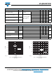
VS-GB50NP120N www.vishay.com Vishay Semiconductors DIODE ELECTRICAL SPECIFICATIONS (TC = 25 °C unless otherwise noted) PARAMETER SYMBOL Diode forward voltage VF Diode reverse recovery time TEST CONDITIONS IF = 50 A trr Diode peak reverse recovery current IRM Diode reverse recovery energy IF = 50 A, VR = 600 V, dI/dt = - 2100 A/μs, VGE = - 15 V MIN. TYP. MAX. TJ = 25 °C - 2.15 - TJ = 125 °C - 2.
VS-GB50NP120N www.vishay.com Vishay Semiconductors 10 10 9 8 Cies Eoff 6 5 C (nF) Eon, Eoff (mJ) 7 Eon 4 1 Coes 3 2 Cres 1 0 0.1 0 10 20 30 40 50 60 70 80 IC (A) 93418_03 0 90 100 5 10 15 20 25 30 35 VCE (V) 93418_06 Fig. 6 - Typical Capacitance vs. Collector to Emitter Voltage Fig. 3 - Switching Loss vs.
VS-GB50NP120N www.vishay.com Vishay Semiconductors 100 90 80 25 °C 70 125 °C IF (A) 60 50 40 30 20 10 0 0 93418_09 0.5 1.0 1.5 2.0 2.5 3.0 3.5 VF (V) Fig. 9 - Typical Forward Characteristics (Diode) 1 Diode IGBT ZthJC (K/W) 0.1 0.01 0.001 0.0001 0.00001 0.0001 0.001 0.01 0.1 1 tp (s) 93418_10 Fig. 10 - Transient Thermal Impedance CIRCUIT CONFIGURATION 6 7 1 2 3 LINKS TO RELATED DOCUMENTS Dimensions Revision: 06-Aug-12 www.vishay.
Legal Disclaimer Notice www.vishay.com Vishay Disclaimer ALL PRODUCT, PRODUCT SPECIFICATIONS AND DATA ARE SUBJECT TO CHANGE WITHOUT NOTICE TO IMPROVE RELIABILITY, FUNCTION OR DESIGN OR OTHERWISE. Vishay Intertechnology, Inc., its affiliates, agents, and employees, and all persons acting on its or their behalf (collectively, “Vishay”), disclaim any and all liability for any errors, inaccuracies or incompleteness contained in any datasheet or in any other disclosure relating to any product.